High density trench FET with integrated Schottky diode and method of manufacture

a diode and trench technology, applied in the direction of diodes, semiconductor devices, electrical apparatus, etc., can solve the problems of reducing the current rating or large die size, and relatively high forward voltage of the body diode. , to achieve the effect of higher doping concentration

Active Publication Date: 2008-11-04
SEMICON COMPONENTS IND LLC
View PDF317 Cites 82 Cited by
  • Summary
  • Abstract
  • Description
  • Claims
  • Application Information

AI Technical Summary

Problems solved by technology

Unfortunately the body diode has relatively high forward voltage and energy is wasted.
The lower forward voltage of the Schottky diode results in improved power consumption.
As a result, the Schottky diodes consume a significant portion of the active area, resulting in lower current ratings or a large die size.

Method used


Image

  • High density trench FET with integrated Schottky diode and method of manufacture
  • High density trench FET with integrated Schottky diode and method of manufacture
  • High density trench FET with integrated Schottky diode and method of manufacture

Examples


Embodiment Construction

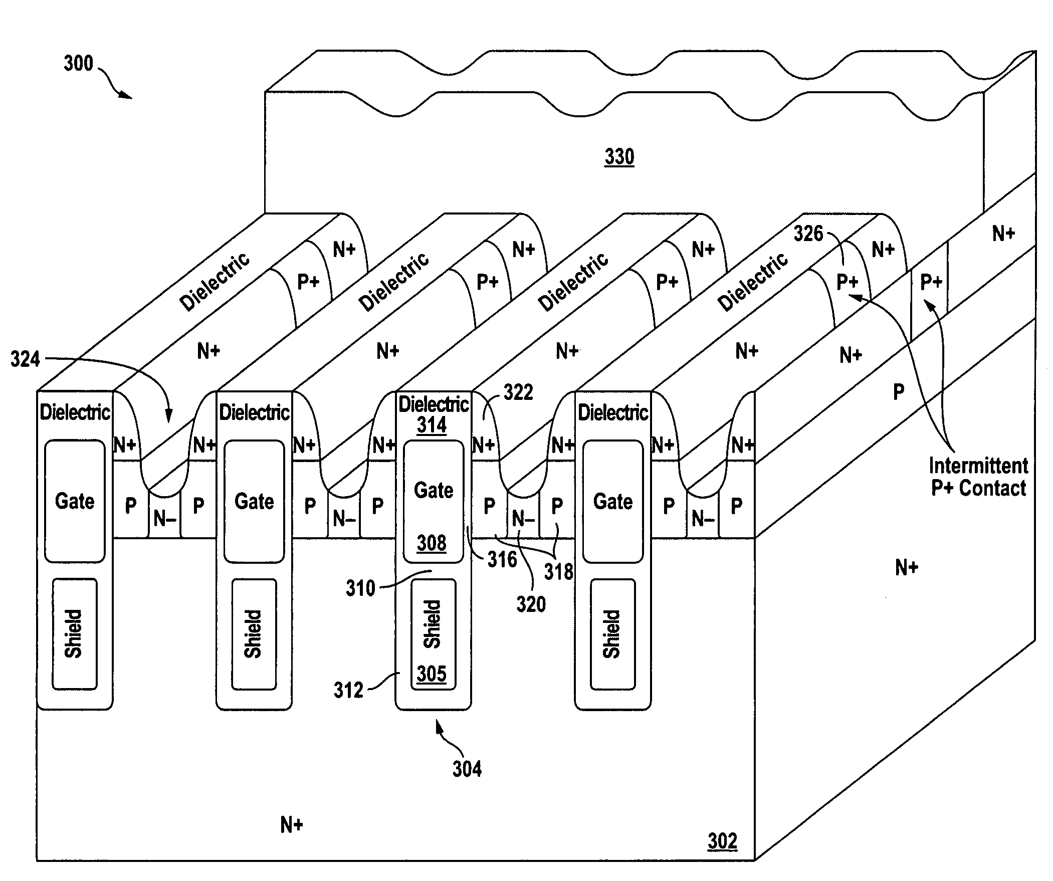
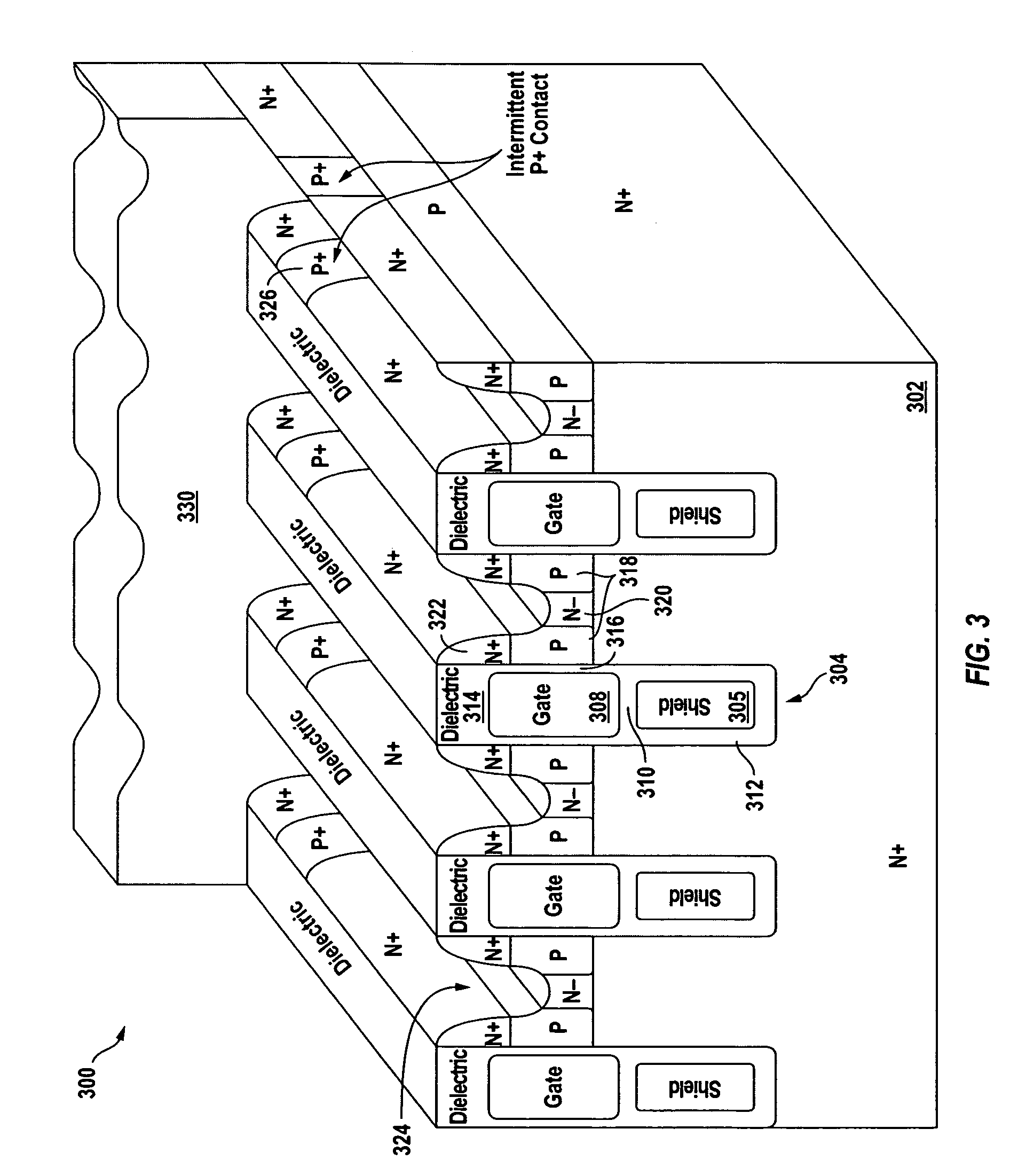
[0028]In accordance with embodiments of the invention, a Schottky diode is optimally integrated with a trench MOSFET in a single cell repeated many times in an array of such cells. Minimal to no active area is sacrificed in integrating the Schottky diode, yet the total Schottky diode area is large enough to handle 100% of the diode forward conduction. The MOSFET body diode thus never turns on, eliminating reverse recovery losses. Further, because of Schottky diode's lower forward voltage drop compared to that of the MOSFET body diode, power losses are reduced.

[0029]Moreover, the Schottky diode is integrated with the MOSFET such that the Schottky contact is formed below the MOSFET source regions. This advantageously diverts the avalanche current away from the source regions toward the Schottky regions, preventing the parasitic bipolar transistor from turning on. The device ruggedness is thus improved. This feature of the invention also eliminates, for the most part, the need for heav...


PUM


Abstract

A monolithically integrated trench FET and Schottky diode includes a pair of trenches terminating in a first silicon region of first conductivity type. Two body regions of a second conductivity type separated by a second silicon region of the first conductivity type are located between the pair of trenches. A source region of the first conductivity type is located over each body region. A contact opening extends between the pair of trenches to a depth below the source regions. An interconnect layer fills the contact opening so as to electrically contact the source regions and the second silicon region. Where the interconnect layer electrically contacts the second silicon region, a Schottky contact is formed.

Description

CROSS-REFERENCES TO RELATED APPLICATIONS[0001]This application is related to the commonly assigned U.S. application Ser. No. 11 / 026,276, filed Dec. 29, 2004, which disclosure is incorporated herein by reference in its entirety for all purposes.BACKGROUND OF THE INVENTION[0002]The present invention relates in general to semiconductor power device technology, and in particular to structures and methods for forming a monolithically integrated trench gate field effect transistor (FET) and Schottky diode.[0003]In today's electronic devices it is common to find the use of multiple power supply ranges. For example, in some applications, central processing units are designed to operate with a different supply voltage at a particular time depending on the computing load. Consequently, dc / dc converters have proliferated in electronics to satisfy the wide ranging power supply needs of the circuitry. Common dc / dc converters utilize high efficiency switches typically implemented by power MOSFETs...

Claims


Application Information

Patent Timeline
Patent Type & Authority Patents(United States)
IPC IPC(8): H01L29/76H01L29/94
CPCH01L29/7813H01L29/66734H01L29/7806H01L29/66727H01L29/0696H01L29/407H01L29/74H01L29/872
Inventor THORUP, PAULCHALLA, ASHOKMARCHANT, BRUCE DOUGLAS
Owner SEMICON COMPONENTS IND LLC
Why Eureka
Try Eureka