

Tri-state circuit using nanotube switching elements
a switching element and tri-state technology, applied in the field of logic circuits, can solve the problems of high power consumption, density and operation speed of mos digital circuits, and limited density of bipolar digital integrated circuits
- Summary
- Abstract
- Description
- Claims
- Application Information
AI Technical Summary
Benefits of technology
Problems solved by technology
Method used
Image

Examples
Embodiment Construction
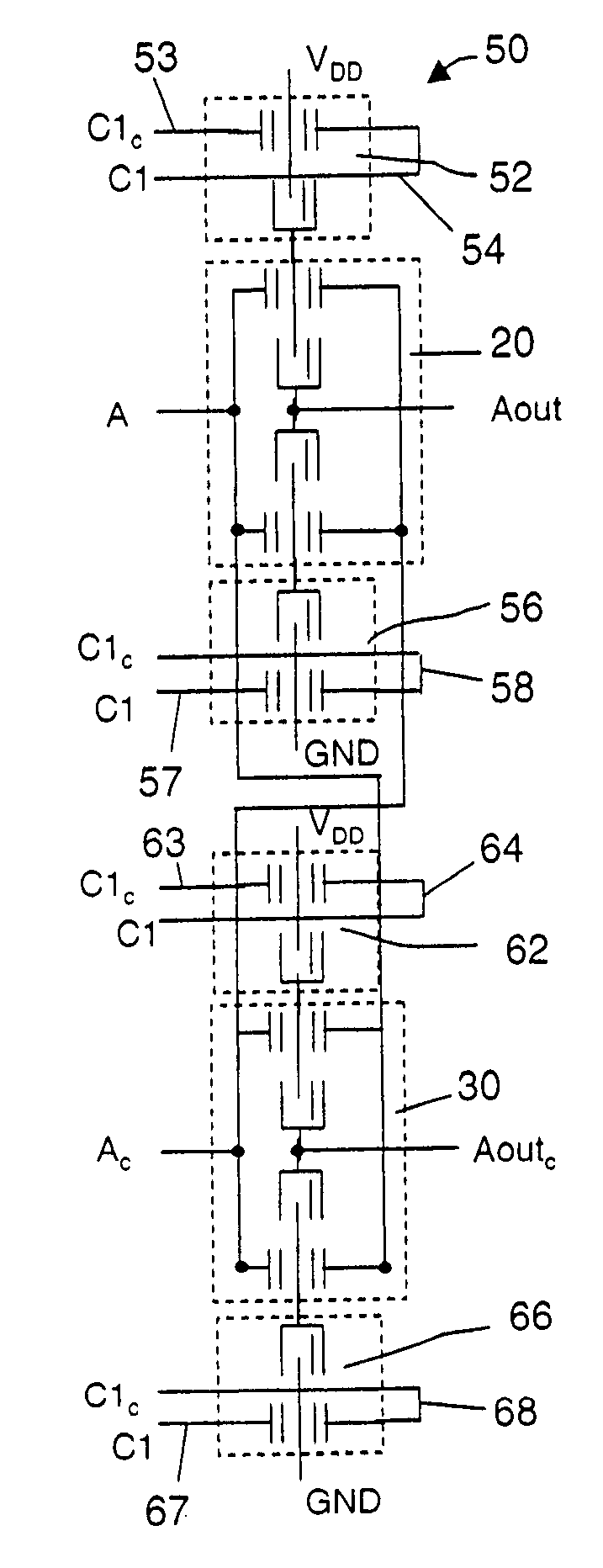
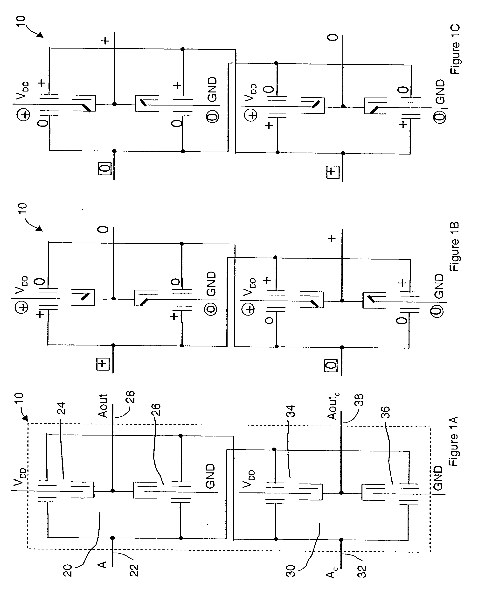
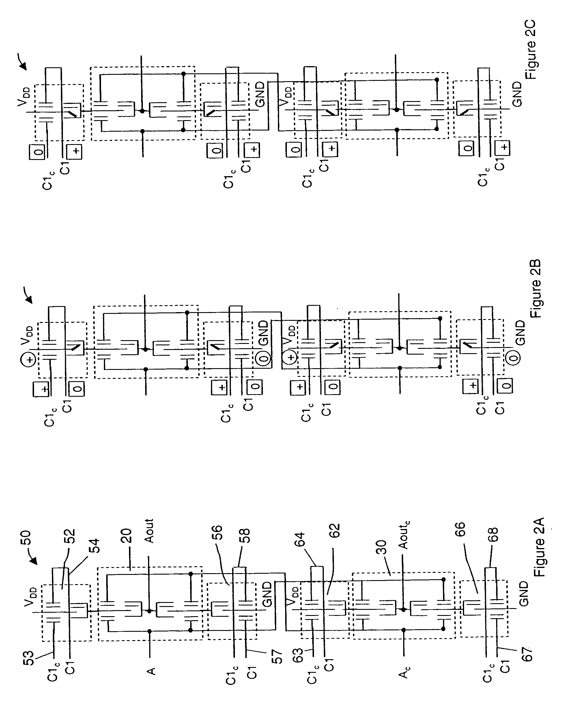
[0053] The present invention provide tri-state nanotube logic circuits constructed from one or more nanotube-switching elements. The use of some embodiments of such devices offers a solution to the CMOS problems of power dissipation and radiation sensitivity. In certain embodiments, the present invention uses electromechanical switches including carbon nanotube channel elements to build complementary nanotube logic. Nanotube-based pull-up and pull-down circuits can be connected to form complementary circuits that only dissipate power when switching. In embodiments of the invention, the circuits are tri-state circuits that have a mode wherein the output can be set to a high-impedance condition. In certain embodiments, the circuits thus combine the benefits of nanotube switching elements with the tri-state feature. For complementary logic circuits, a pull-up tri-state element and a pull-down tri-state element are provided. In certain embodiments, the pull-up tri-state element is dispo...
PUM
 Abstract
Description
Claims
Application Information