Eureka AIR delivers breakthrough ideas for toughest innovation challenges, trusted by R&D personnel around the world.

Deposition methods, and deposition apparatuses

Active Publication Date: 2006-11-16
MICRON TECH INC
View PDF9 Cites 16 Cited by
  • Summary
  • Abstract
  • Description
  • Claims
  • Application Information

AI Technical Summary

Benefits of technology

[0087] Among the advantages of the apparatuses and methods of the present invention relative to the prior art apparatuses and methods discussed above with reference to FIGS. 4-7, are that the boats 62 tend to be expensive and are a consumed material. In contrast, reaction chamber modification to accomplish the methods of the present invention can be done economically. Also, the heated surfaces utilized in methodologies of the present invention may last much longer than the boats utilized in the prior art methodologies.

Problems solved by technology

However, the distinction between ALD and CVD processes often blurs in actual applications so that processes that primarily proceed by ALD may still have some CVD-type contribution.
Nevertheless, such an imperfect monolayer is still a monolayer in the context of this document.
The second species might only bond to the first species and thus may also be self-limiting.
Accordingly, operating outside the traditional temperature and pressure ranges may risk formation of defective monolayers.
It can be desired to process a batch of multiple semiconductor wafers in order to increase throughput of a fabrication process, however, such can also lead to difficulties in forming uniform thicknesses of material across the semiconductor wafers.
Even if relatively slow reacting precursors are utilized, there can be problems with the uniformity of deposition achieved across a semiconductor wafer substrate surface during a batch CVD process.
Such non-uniformity of deposition of coating 50 can significantly complicate further processing.
A problem with the processing of FIGS. 4-7 is that the boat is an added expense and has a limited lifetime.
However, ALD processes frequently have a CVD-type component, and such component can lead to the problematic edge build-up comparable to the build-up discussed above with reference to FIG. 3 for a CVD process.
Although the problems of FIG. 3 are discussed relative to batch processes, it is to be understood that similar problems can also occur in single wafer processes.
The problem of FIG. 3 is but one of several problems that can occur during utilization of a deposition apparatus, such as the exemplary apparatus of FIGS. 1 and 2.
Another problem that can occur is that precursor can become depleted within the flow 30 as the flow migrates through the reaction chamber of the apparatus.

Method used


Image

  • Deposition methods, and deposition apparatuses
  • Deposition methods, and deposition apparatuses
  • Deposition methods, and deposition apparatuses

Examples


Embodiment Construction

[0048] This disclosure of the invention is submitted in furtherance of the constitutional purposes of the U.S. Patent Laws “to promote the progress of science and useful arts” (Article 1, Section 8).

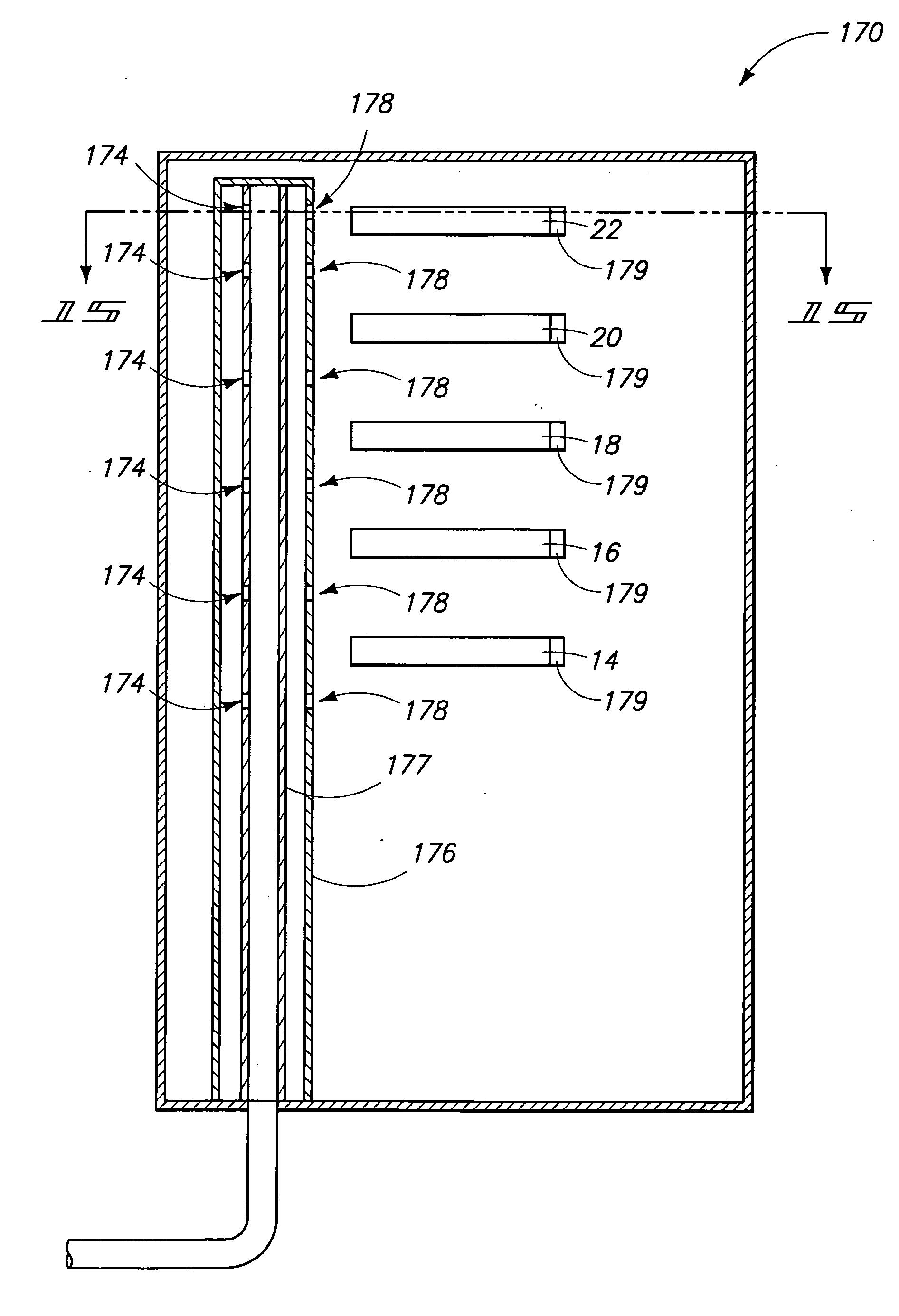
[0049] The invention includes incorporation of at least one heated surface into a deposition chamber so that injected fluids interact with the heated surface prior to reaching semiconductor wafer substrates. The semiconductor wafer substrates are heated to conventional temperatures for a deposition process, and the heated surface is heated to at least about the temperature of the semiconductor wafer substrates. Specifically, the heated surface is heated to a sufficient temperature so that undesired thermal reactions that would occur proximate the heated substrates instead occur proximate the heated surface. Thus, the reference to the heated surface being heated to “at least about the temperature of the semiconductor substrates” (or alternatively, at least approximately the temperature o...


PUM

PropertyMeasurementUnit
Temperatureaaaaaaaaaa
Distanceaaaaaaaaaa
Semiconductor propertiesaaaaaaaaaa

Abstract

The invention includes deposition methods and apparatuses which can be utilized during atomic layer deposition or chemical vapor deposition. A heated surface is provided between a stack of semiconductor substrates and a precursor inlet, and configured so that problematic side reactions occur proximate the heated surface rather than proximate the semiconductor substrates. The precursor inlet can be one of a plurality of precursor inlets, and the heated surface can be one of a plurality of heated surfaces.

Description

TECHNICAL FIELD [0001] The invention pertains to deposition methods and to deposition apparatuses. In particular aspects, the invention pertains to atomic layer deposition methods and apparatuses, and / or to chemical vapor deposition methods and apparatuses. BACKGROUND OF THE INVENTION [0002] Some background on ALD and CVD may assist the reader in understanding the present disclosure. ALD is generally considered to include processes in which precursors alternately react at an exposed surface in a self-limiting manner with no direct interaction except for the exposed surface. CVD is generally considered to include processes in which one or more precursors react above a surface to form a material that ultimately deposits over the surface in a continuous deposition or not self-limiting manner. However, the distinction between ALD and CVD processes often blurs in actual applications so that processes that primarily proceed by ALD may still have some CVD-type contribution. [0003] Typicall...

Claims


Application Information

Patent Timeline
IPC IPC(8): H01L21/44
CPCC23C16/45546C23C16/45578C23C16/4557C23C16/458C23C16/46
Inventor WEIMER, RONALD A.
Owner MICRON TECH INC
Why Eureka
Eureka Blog
Learn More