Thermal electron emission backlight device

a backlight device and electron emission technology, applied in the manufacture of electric discharge tubes/lamps, luminescnet screens, electric discharge tubes/lamps, etc., can solve the problems of high cost, complicated manufacturing process of backlights, and insufficient environmental protection of cold cathode electrode tubes. achieve the effect of high brightness

Inactive Publication Date: 2006-11-23
SAMSUNG SDI CO LTD
View PDF9 Cites 8 Cited by
  • Summary
  • Abstract
  • Description
  • Claims
  • Application Information

AI Technical Summary

Benefits of technology

[0007] The present invention relates to a thermal electron emission backlight device having high brightn

Problems solved by technology

However, the cold cathode cold cathode electrode tube is not environmentally friendly since the cold cathode electrode tube uses mercury.
In addition, it is becoming expensive since the structure is more complicated as it is bigger by using a light guide plate.
A triode structure field emission device, as disclosed in U.S. Pat. No. 5,760,858, can solve the above problem, but the manufacturing

Method used


Image

  • Thermal electron emission backlight device
  • Thermal electron emission backlight device
  • Thermal electron emission backlight device

Examples


Embodiment Construction

[0025] the thermal electron emission backlight device according to the present invention will now be described more fully with reference to the accompanying drawings in which exemplary embodiments of the invention are shown. In the drawings, the thicknesses of layers and regions are exaggerated for clarity.

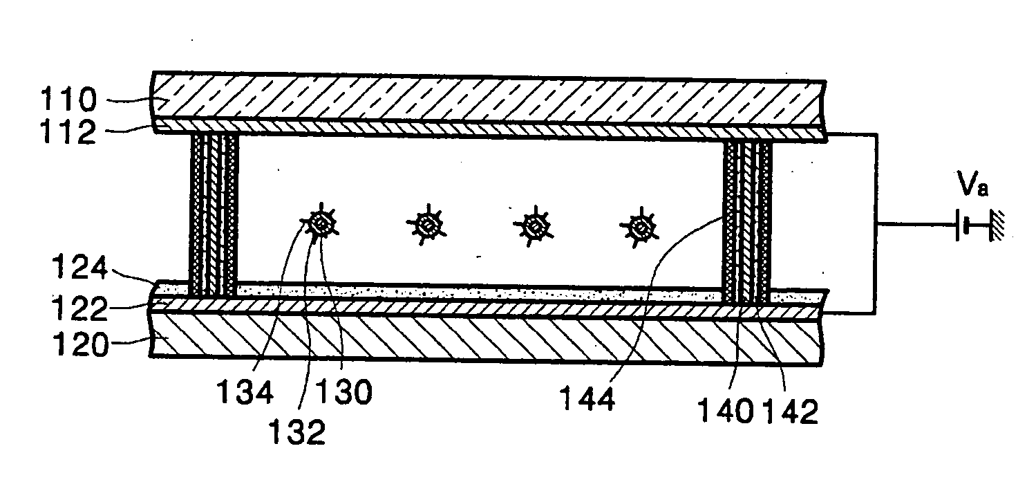
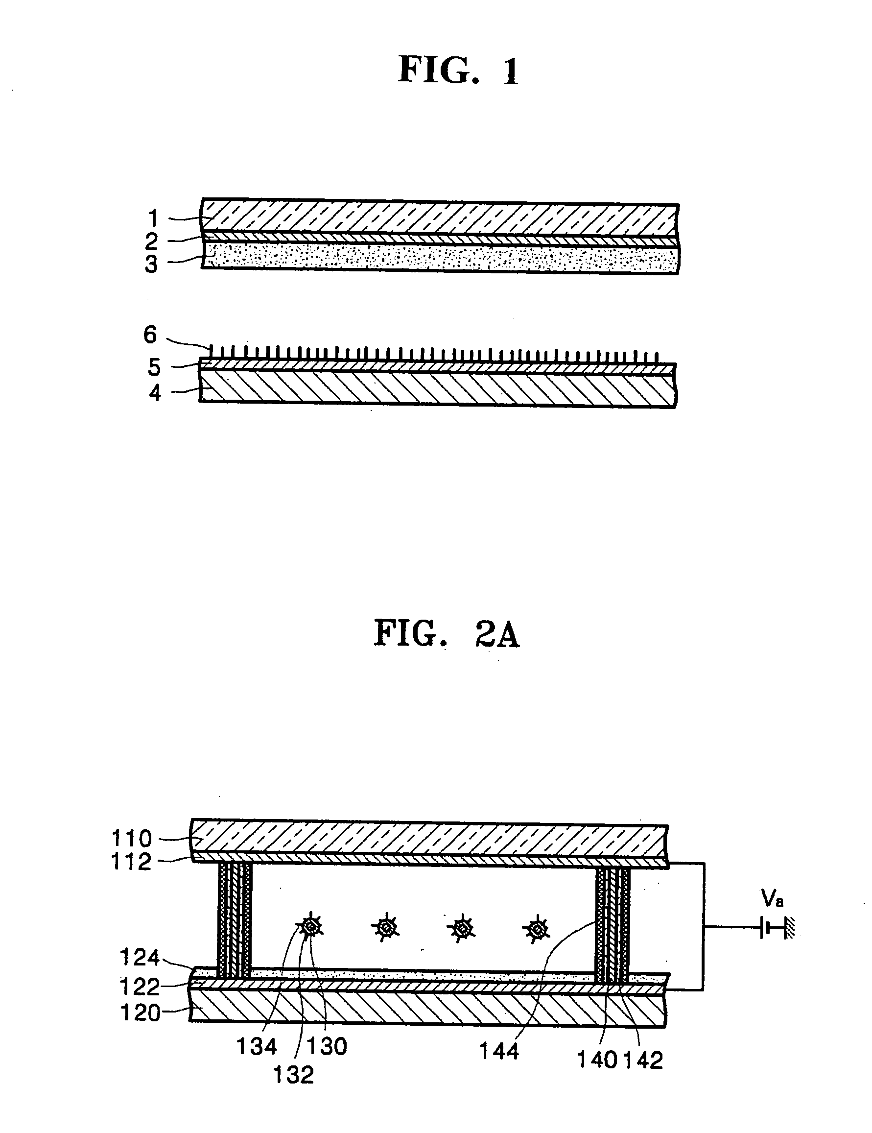
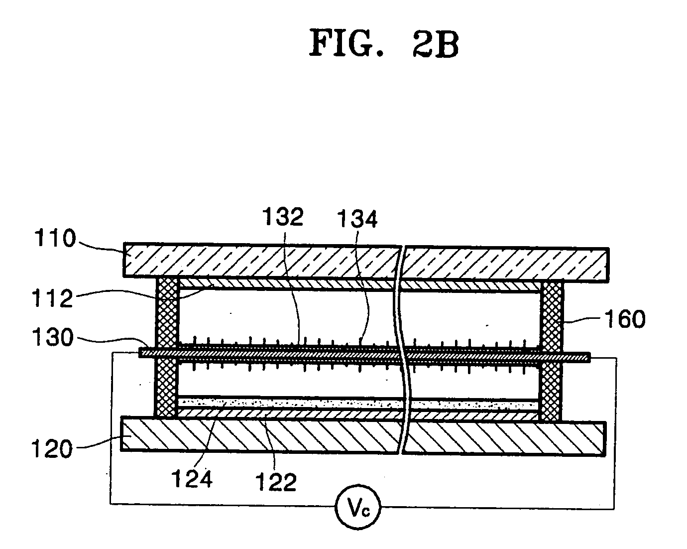
[0026]FIG. 1 is a cross-section view of a backlight device for a liquid crystal display (LCD).

[0027] Referring to FIG. 1, a spacer (not shown) is disposed between a front substrate 1 and a rear substrate 4. Walls (not shown) between the front substrate 1 and the rear substrate 4 are sealed. A cathode electrode 5 having a plate type shape or a stripe shape is formed on the rear substrate 4. A field emission source 6, such as carbon nanotubes (CNTs), is formed on the cathode electrode 5. An anode electrode 2, which is a transparent electrode, is formed on the front substrate 1. A phosphor layer 3 is coated on the anode electrode 2.

[0028] When a predetermined voltage is applied to...


PUM


Abstract

A thermal electron emission backlight device comprises: a first substrate and a second substrate disposed in parallel and separated by a predetermined distance from each other; a first anode electrode and a second anode electrode facing the first anode electrode, the first and second anode electrodes being formed on inner surfaces of the first substrate and the second substrate, respectively; cathode electrodes disposed at predetermined intervals and in parallel with each other between the first substrate and the second substrate; a phosphor layer formed on the second anode electrode; and a plurality of spacers disposed between the first substrate and the second substrate so as to maintain the predetermined distance therebetween. When a predetermined voltage is applied to the cathode electrodes, thermal electrons are emitted from the cathode electrodes.

Description

CLAIM OF PRIORITY [0001] This application makes reference to, incorporates the same herein, and claims all benefits accruing under 35 U.S.C.§ 119 from an application for FIELD EMISSION BACKLIGHT DEVICE EMITTING THERMAL ELECTRON earlier filed in the Korean Intellectual Property Office on the 23rd of May 2005 and there duly assigned Ser. No. 10-2005-0043158. BACKGROUND OF THE INVENTION [0002] 1. Technical Field [0003] The present invention relates to a thermal electron emission backlight device and, more particularly, to a back light device that emits white light by exciting a phosphor layer using thermal electrons. [0004] 2. Related Art [0005] A backlight device which emits white light is installed on a rear surface of a liquid crystal display (LCD). A plasma type cold cathode electrode tube has been mainly used as the backlight. However, the cold cathode cold cathode electrode tube is not environmentally friendly since the cold cathode electrode tube uses mercury. In addition, it is...

Claims


Application Information

Patent Timeline
IPC IPC(8): H01J63/04H01J1/62
CPCH01J63/04H01J63/02H01J9/02H01J9/242H01J9/025
Inventor CHOI, JUN-HEECHUNG, DEUK-SEOKSONG, BYONG-GWONZOULKARNEEV, ANDREIBAIK, CHAN-WOOKKIM, HA-JONGSHIN, MOON-JINKANG, HO-SUK
Owner SAMSUNG SDI CO LTD
Why Eureka
Try Eureka