Manufacturing method of thin film transistor

Inactive Publication Date: 2006-11-23
SEMICON ENERGY LAB CO LTD
View PDF32 Cites 46 Cited by
  • Summary
  • Abstract
  • Description
  • Claims
  • Application Information

AI Technical Summary

Benefits of technology

[0023] Further, by forming an electrode of a thin film transistor in a circular shape (circular electrode), a wire can be lead out from all directions of the electrode. As a result, freedom of a wiring layout can be improved and various problems caused by leading wires (for example, electrical problems such as impedance (wire resistance, wire capacitance, wire inductance) and reflection (mainly for high frequency) generated when the wire is bent, and mechanical problems such as peeling off of a film due to the stress which rather concentrates at an edge portion of the film) can be improved. (The aforementioned circular electrode does not necessarily have a perfect circle shape. That is, the electrode may have an oval shape or the like).
[0024] By forming each electrode in a closed shape like a loop, a channel portion having a channel length (L) with uniform lengths in a direction from a source electrode to a drain electrode can be formed (it is difficult to form uniform channel lengths in an electrode shape of a thin film transistor formed by a conventional droplet discharge method since a landed droplet cannot form a straight line). Moreover, a channel width (W) can be formed with less error of the design value than the conventional method (a thin film transistor formed by the conventional method tends to have error of the design value due to an effect on its edge portions). Therefore, by forming a structure w

Problems solved by technology

Furthermore, patterning of an electrode, a wire, and the like requires exposure of a resist to light using a mask, which leads to problems in that the number of steps is increased and that efficiency and environment are both affected by the waste liquid.
Further, there are many unnecessary areas in the electrode, which ends in occupying a wide area for the thin film transistor.
The aforementioned problems are notably present in a thin film transistor having a conventional shape, which is formed by a method using no mask (maskless process) in particular.
In the case of forming a circular thin film transistor having a circular electrode by using a mask as in a conventional way in order to solve the aforementioned problems, it is difficult to form each electrode into a perfect circular shape.
Originally, it is difficult to form a perfect curve in forming a circular shape by using a photo mask

Method used


Image

  • Manufacturing method of thin film transistor
  • Manufacturing method of thin film transistor
  • Manufacturing method of thin film transistor

Examples


embodiment mode 1

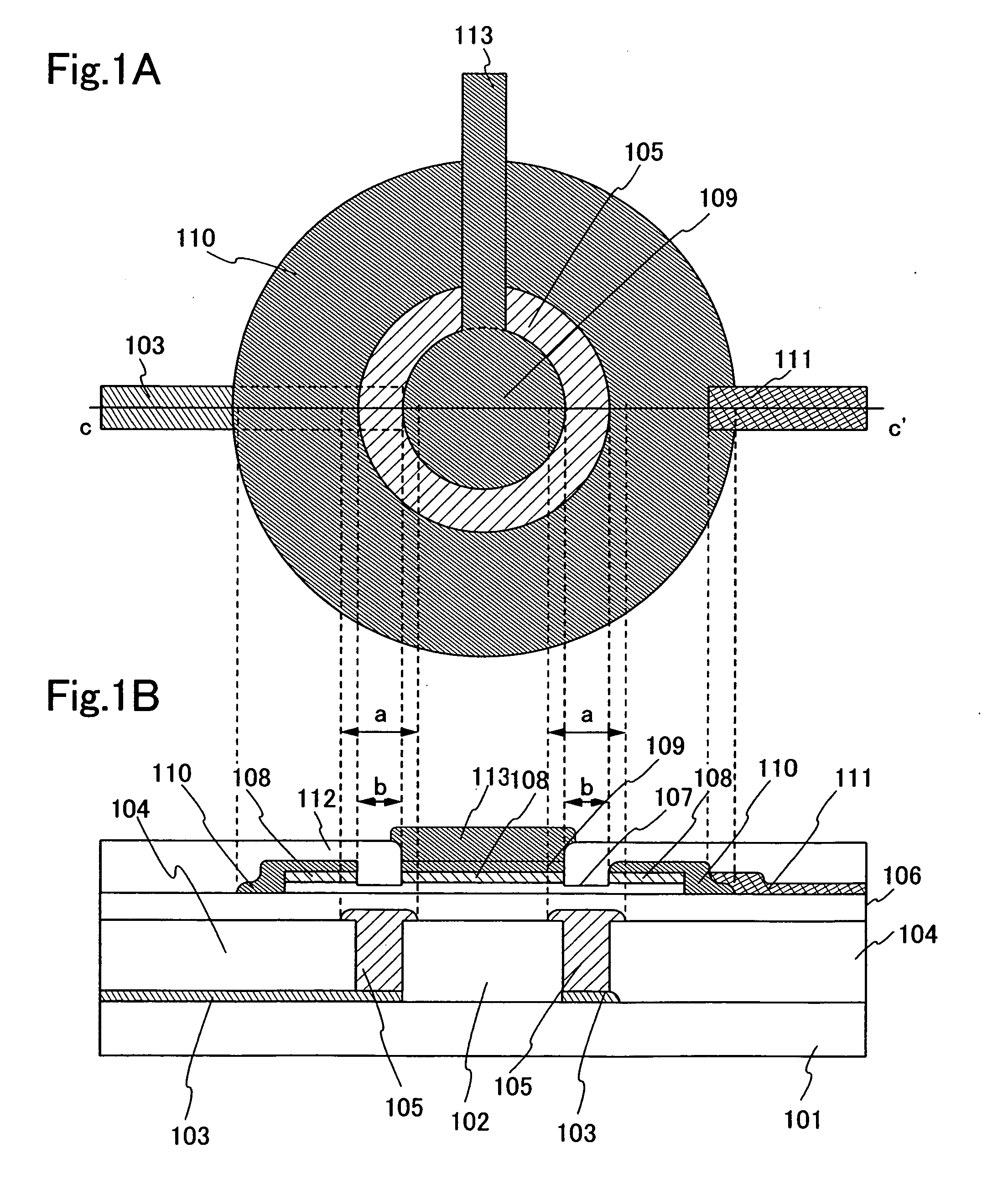
[0058] Description is made with reference to FIGS. 1A to 4C on structures and a manufacturing method of a circular thin film transistor of the invention.

[0059]FIG. 1A is a top plan view of a circular thin film transistor of the invention and FIG. 1B is a cross sectional view thereof.

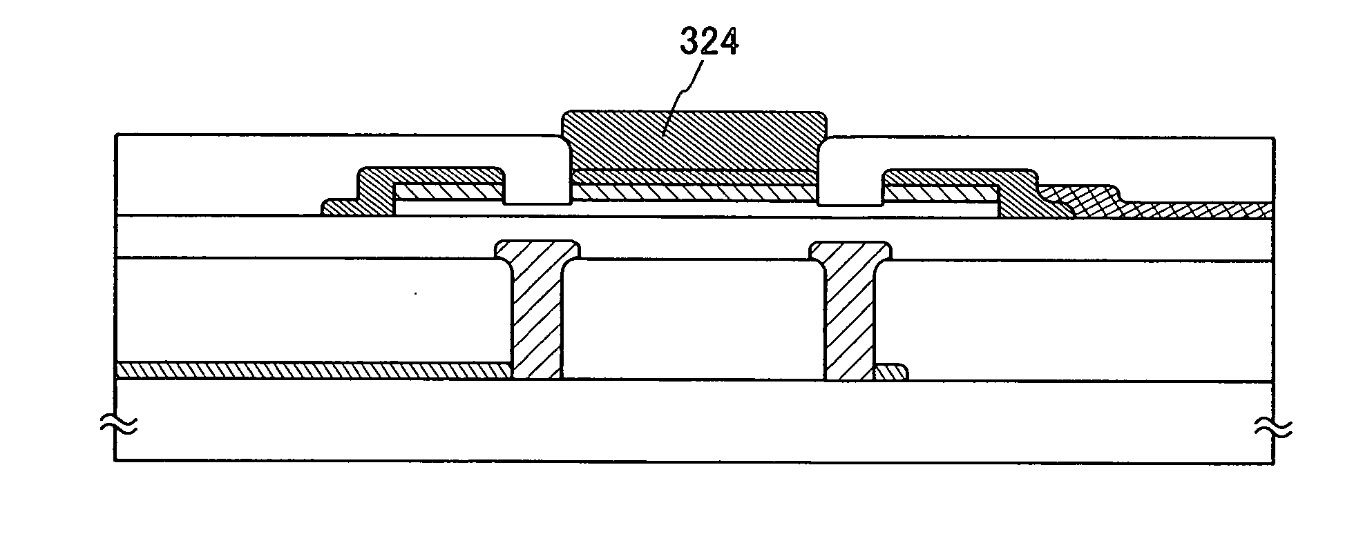
[0060] As shown in FIG. 1B, a first insulating layer 102 and a first conductive layer 103 are formed over a substrate 101, and then a second insulating layer 104 and a second conductive layer 105 are formed. It is to be noted that the first conductive layer 103 functions as a gate wire here and the second conductive layer 105 functions as a gate electrode. Note that the second conductive layer 105 is covered with a third insulating layer 106.

[0061] Further, semiconductor layers 107 and 108 are formed as active layers over the third insulating layer 106. A third conductive layer 109 which functions as a source electrode is formed over the semiconductor layer 108 provided at a center portion of the circ...

embodiment mode 2

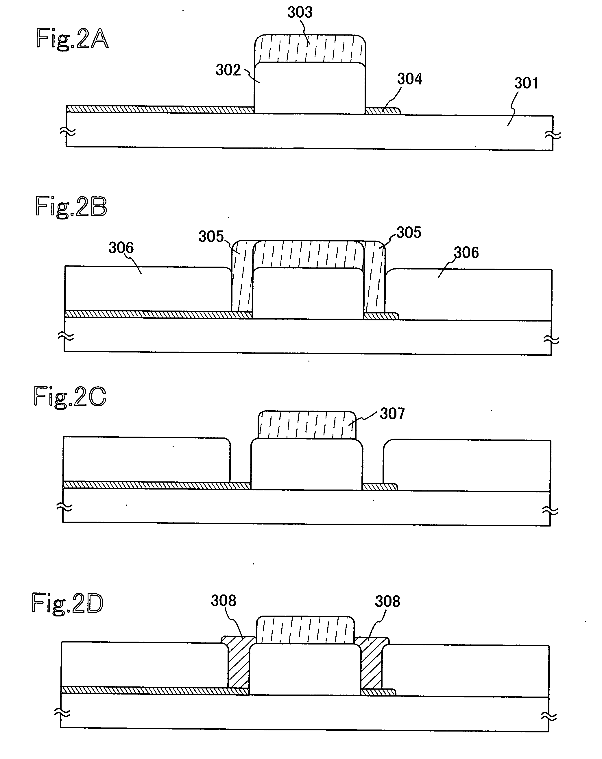
[0095] A structure and a manufacturing method of a circular thin film transistor of the invention are described with reference to FIGS. 5A to 7B. It is to be noted in Embodiment Mode 2 that the method described in Embodiment Mode 1 can be used in the case of using a liquid-repellent application method. Further, the materials described in Embodiment Mode 1 can be used as materials used for forming insulating layers (including first to fourth insulating layers in Embodiment Mode 2), liquid-repellent layers (including first to fifth liquid-repellent layers in Embodiment Mode 2), and conductive layers (including first to fifth conductive layers in Embodiment Mode 2).

[0096]FIG. 5A is a top plan view of a circular thin film transistor of the invention and FIG. 5B is a cross sectional view thereof.

[0097] As shown in FIG. 5B, a first insulating layer 202 and a first conductive layer 203 are formed over a substrate 201, and a second insulating layer 204 and a second conductive layer 205 ar...

embodiment mode 3

[0112] A structure and a manufacturing method of a circular thin film transistor of the invention will be described with reference to FIGS. 8A to 11B. It is to be noted in Embodiment Mode 3 that the method described in Embodiment Mode 1 can be used in the case of using a liquid-repellent application method. Further, the materials described in Embodiment Mode 1 can be used as materials used for forming insulating layers (including first to fourth insulating layers in Embodiment Mode 3), liquid-repellent layers (including first to sixth liquid-repellent layers in Embodiment Mode 3), and conductive layers (including first to sixth conductive layers in Embodiment Mode 3).

[0113]FIG. 8A is a top plan view of a circular thin film transistor of the invention and FIG. 8B is a cross sectional view thereof.

[0114] As shown in FIG. 8B, a first insulating layer 1402 and a first conductive layer 1403 are formed over a substrate 1401, and a second insulating layer 1404 and a second conductive lay...


PUM


Abstract

The invention provides a manufacturing method of a circular thin film transistor of which shape is more controlled than the conventional case, while simplifying the steps and reducing the manufacturing time and cost by forming a circular thin film transistor by a maskless process such as a droplet discharge method. In the invention, a circular thin film transistor having a circular electrode is formed by stacking concentric circular thin films over a substrate by a maskless process such as a droplet discharge method. Moreover, a circular thin film transistor having a circular semiconductor layer may be formed by stacking concentric circular thin films over a substrate by a maskless process such as a droplet discharge method.

Description

BACKGROUND OF THE INVENTION [0001] 1. Field of the Invention [0002] The invention relates to a thin film transistor (TFT) having a circular electrode (hereinafter referred to as a circular thin film transistor (TFT)), a semiconductor device including the circular thin film transistor, and a manufacturing method thereof. It is to be noted that a semiconductor device corresponds to a thin film transistor substrate including a thin film transistor over a substrate, a liquid crystal panel substrate or a liquid crystal module substrate including a thin film transistor and liquid crystals over a substrate, an EL (Electro Luminescence) panel substrate or an EL module substrate including a thin film transistor and a light emitting element over a substrate, a liquid crystal panel including a thin film transistor and liquid crystals over a substrate which are sealed by a sealing material, an EL panel including a thin film transistor and a light emitting element over a substrate which are seal...

Claims


Application Information

Patent Timeline
IPC IPC(8): G03B21/62
CPCH01L29/41733H01L29/42384Y10T428/24421H01L29/66765H01L29/66757
Inventor HIROSE, ATSUSHI
Owner SEMICON ENERGY LAB CO LTD
Why Eureka
Try Eureka