Semiconductor device having shallow trench isolation structure and method of manufacturing the same

a technology of isolation structure and semiconductor, which is applied in the direction of semiconductor devices, basic electric elements, electrical appliances, etc., can solve the problems of deteriorating performance of unit devices, becoming more difficult to form sti structures, and unable to ensure a sufficient process margin in an effective region of an active region, so as to improve isolation properties and improve trench depth variation , good gap filling properties

Inactive Publication Date: 2006-11-23
SAMSUNG ELECTRONICS CO LTD
View PDF13 Cites 50 Cited by
  • Summary
  • Abstract
  • Description
  • Claims
  • Application Information

AI Technical Summary

Benefits of technology

[0008] The present invention provides a semiconductor device having an isolation structure that can provide a stable isolation property, effectively prevent a hot electron induced punchthrough (HEIP) effect, and increase the region of an active region.
[0009] The present invention also provides a method of manufacturing a semiconductor device, capable of restraining consumption of an active region by oxidation, providing easy trench filling, and providing a stable isolation structure.
[0016] The upper trench has a good gap filling property when filling an STI trench with an insulating layer for isolation. Additionally, by forming a void with a lower dielectric constant than that of the conventional oxide layer inside the lower trench according to deposition conditions of an insulating layer for isolation, an isolation property can be improved. An isolation region can improve the depth variation of trench for isolation formed on a various positions of the entire surface in a wafer by forming a lower trench to have a substantially curved or round-shaped cross-sectional profile using an isotropic dry etching process. The region of an active region increases and an electric property is improved by forming a spacer of an oxide layer in an inner wall of the upper trench.

Problems solved by technology

Also, because CMOS devices are manufactured using 70 nm technology or less, it becomes more difficult to form their STI structures.
Consequently, it becomes more difficult to ensure an effective region of an active region for a sufficient process margin.
As a result, the performance of a unit device deteriorates and a malfunction of a device may occur.

Method used


Image

  • Semiconductor device having shallow trench isolation structure and method of manufacturing the same
  • Semiconductor device having shallow trench isolation structure and method of manufacturing the same
  • Semiconductor device having shallow trench isolation structure and method of manufacturing the same

Examples


Embodiment Construction

[0026] Some embodiments of the present invention will now be described more fully with reference to the accompanying drawings, in which exemplary embodiments of the invention are illustrated. One skilled in the art should appreciate that elements in the figures are illustrated for simplicity and clarity and have not necessarily been drawn to scale. For example, the dimensions of some of the elements in the figures may be exaggerated relative to other elements to help improve the understanding of the embodiments of the present invention.

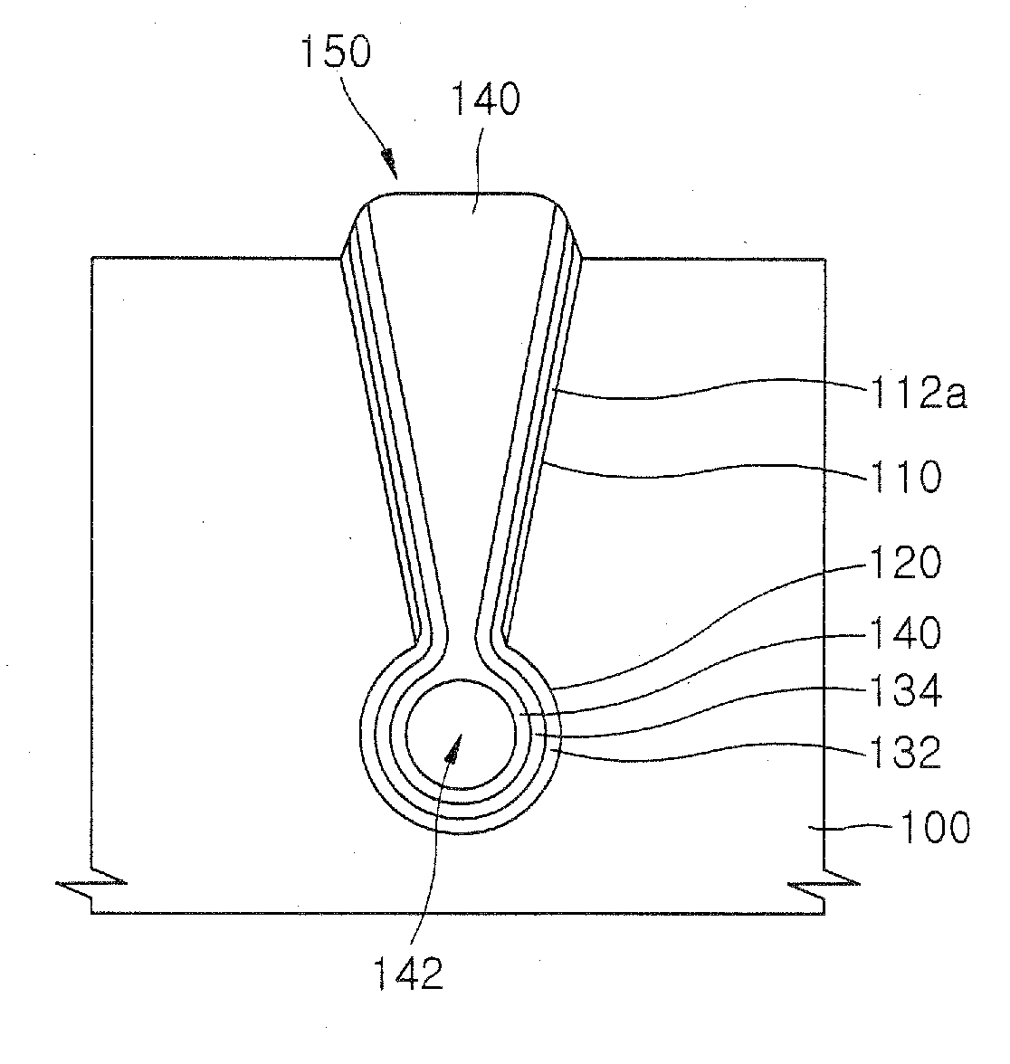
[0027] An isolation layer defining an active region on a semiconductor substrate is formed using an STI technology. The isolation layer is formed inside an STI trench formed by etching a region of a semiconductor substrate. The STI trench includes an upper trench and a lower trench. The lower trench is connected to the upper trench via the bottom of the upper trench and has a substantially curved or round-shaped cross-sectional profile. An insulating...


PUM


Abstract

In one embodiment, a semiconductor device has an active region defined by an isolation layer formed inside an STI trench that includes an upper trench and a lower trench having a substantially curved cross-sectional profile under the upper trench so that the lower trench is in communication with the upper trench. Since the upper trench has a sidewall tapered with a positive slope, a good gap filling property can be obtained when filling the upper trench with an insulating layer. By forming a void in the lower trench, a dielectric constant at the bottom of the isolation layer is lower than a dielectric constant at an oxide layer, thereby improving the isolation property. The isolation layer includes a first insulating layer formed inside only the upper trench and covering an inner wall of the upper trench in the form of a spacer.

Description

CROSS-REFERENCE TO RELATED PATENT APPLICATION [0001] This application claims the benefit of Korean Patent Application No. 10-2005-0041761, filed on May 18, 2005, in the Korean Intellectual Property Office, the disclosure of which is incorporated herein in its entirety by reference. [0002] 1. Field of the Invention [0003] The present invention relates to a semiconductor integrated circuit device and a method of its manufacture, and more particularly, to a semiconductor device having a shallow trench isolation structure (STI) and a method of its manufacture. [0004] 2. Description of the Related Art [0005] As semiconductor integration increases, an isolation technology for electrically isolating adjacent devices becomes more important. A shallow trench isolation (STI) formation process is a widely used isolation technology in manufacturing of high integration semiconductor devices. The STI formation process is used to form a trench defining an active region on a semiconductor substrate...

Claims


Application Information

Patent Timeline
Patent Type & Authority Applications(United States)
IPC IPC(8): H01L21/336H01L29/76
CPCH01L21/76232H01L21/76
Inventor LEE, SUNG-SAMJIN, GYO-YOUNGKIM, YUN-GI
Owner SAMSUNG ELECTRONICS CO LTD
Why Eureka
Try Eureka