Quantum dot intermediate band infrared photodetector

a quantum dot and infrared technology, applied in the field of infrared photodetectors, can solve the problems of reducing the detectivity (capability to distinguish signals from noise) of the photodetector, unable to absorb light at normal incidence, and unable to detect light in the photovoltaic mod

Inactive Publication Date: 2006-11-30
UNIV MADRID POLITECNICA +1
View PDF13 Cites 37 Cited by
  • Summary
  • Abstract
  • Description
  • Claims
  • Application Information

AI Technical Summary

Benefits of technology

[0008] The invention described here combines the best of both type of the above described devices. From one side, it is conceived to operate in the photovoltaic mode. On the other hand, the use of quantum dots allows tuning the wavelength of detection. For this combination of features to be possible, the invention exploits the physical properties predicted in the literature for intermediate band materials. These are characterised by the existence of an intermediate electronic band between what otherwise would be a conventional semiconductor band gap. Intermediate band materials are still mostly a theoretical concept. Some papers, however, have appeared in the literature proposing its synthesis by means of GaxAsTi1-x, II-Ox-VI1-x highly mismatched alloys and even quantum dots. In some cases, some preliminary experimental results have been provided demonstrating the existence of this intermediate band.

Problems solved by technology

A specific draw-back of using quantum wells is that, due to optical selection rules, the absorption of light at normal incidence is not possible, but that can be amended by using quantum dots.
A general draw-back of these photo-detectors is that they do not allow for detection of light in the photovoltaic mode (that is, without, the application of a voltage between device terminals).
This degrades the detectivity (capability to discriminate signal from noise) of the photo-detector and requires the device to be cooled to improve it.
Nevertheless, detection of light in the photovoltaic mode has been reported, although it is considered accidental and the physical reasons for it are not well understood in the literature.
However, only a few semiconductors compounds become available.
Conversely, the detectors based on low semiconductor structures are not conceived to operate in the photovoltaic mode and, therefore, have a potentially worse detectivity.

Method used


Image

  • Quantum dot intermediate band infrared photodetector
  • Quantum dot intermediate band infrared photodetector
  • Quantum dot intermediate band infrared photodetector

Examples


Embodiment Construction

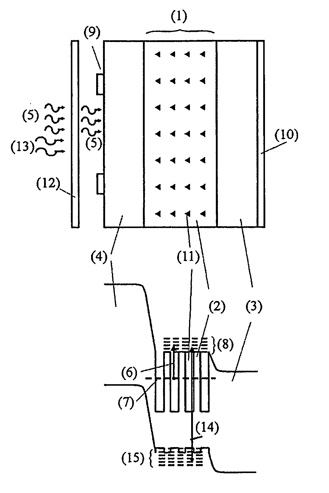
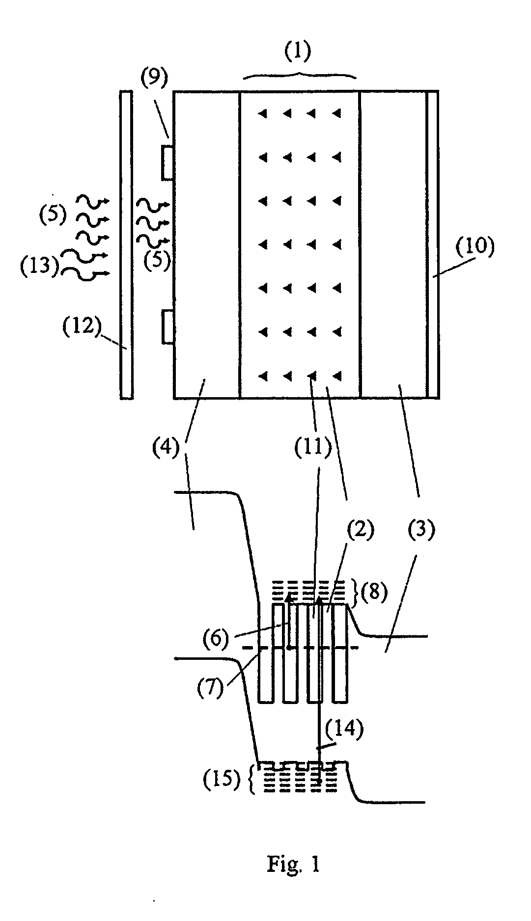
[0024] The invention is also referred to herein as “quantum dot intermediate band infrared photodetector” (QDIB-IR). FIG. 1 shows its basic structure. It comprises a semiconductor region (1) with quantum dots (11) embeded in it and sandwiched between two semiconductor regions, called “emitters.” One of these emitters is of p type (4) and the other is of n type (3). Metal contacts, (9) and (10), are placed on these emitters. The contact located at the front side (9), that is, the side to receive the IR radiation (5), must not cover completely this area in order to allow radiation to come through. Preferably, it should be in the form of a grid.

[0025] The material that constitutes the dots (11) is called “dot material,” and the material that surrounds it, “barrier material” (2). These are made of different semiconductors, characterised usually by different band gaps. When properly chosen, they can lead to a simplified band diagram, also illustrated in FIG. 1, but with some more detail...


PUM


Abstract

An infrared photodetector containing a region of semiconductor quantum dots (1), n type doped in the barrier region (2), and sandwiched between respective layers of semiconductors of n type (3) and p type (4). When infrared photons (5) are absorbed, they create electronic transitions (6) from the confined states in the dots (7) to the conduction band (8). This causes the appearance of a voltage between device p (9) and n (10) contacts or the production of an electrical current. In either way, the detection of the infrared light is possible. A low band-pass filter (12) prevents high energy photons (13) from entering the device and causing electronic transitions (14) from the valence (15) band to the conduction band (8).

Description

TECHNICAL FIELD [0001] This invention relates to the art of infrared photo-detectors, and in particular to semiconductor photo-detectors for detecting infrared radiation. BACKGROUND ART [0002] Infrared photo-detectors are traditionally classified into thermal and photon devices. In thermal devices, the detection of radiation is based on the change of temperature that the absorption of infrared (IR) radiation causes in some sensitive component (gas, resistor, thermocouple, piezoelectric material) of the detector. This change modifies some physical property of the component, which is the one triggering the detection. Examples of these are the pyroelectric detectors, Golay cell detectors, thermopiles and bolometers. [0003] The present invention relates to photon devices characterised by the absorption of IR radiation and the consequent transition of electrons from a lower energy state to a higher energy state. Known IR photon photo-detectors are based either on the use of low band gap ...

Claims


Application Information

Patent Timeline
Patent Type & Authority Applications(United States)
IPC IPC(8): H01L31/00
CPCB82Y10/00B82Y20/00H01L27/1446Y02E10/544H01L31/035236H01L31/105H01L31/0304Y02E10/50Y02P70/50H01L31/035272H01L31/06H01L31/101
Inventor VEGA, ANTONIO MARTILOPEZ, ANTONIO LUQUEMARTINEZ, NAIR LOPEZDIAZ, ENRIQUE CANOVASFERNANDEZ, ELISA ANTOLINSTANLEY, COLIN
Owner UNIV MADRID POLITECNICA
Why Eureka
Try Eureka