OLED electron-transporting layer

a technology of electron transport layer and oled, which is applied in the direction of organic semiconductor devices, discharge tube luminescnet screens, natural mineral layered products, etc., can solve the problems of insufficient luminous efficiency of oled, inability to inject electrons from the cathode into the lel, and inability to achieve high luminous efficiency

Inactive Publication Date: 2006-11-30
EASTMAN KODAK CO
View PDF19 Cites 63 Cited by
  • Summary
  • Abstract
  • Description
  • Claims
  • Application Information

AI Technical Summary

Benefits of technology

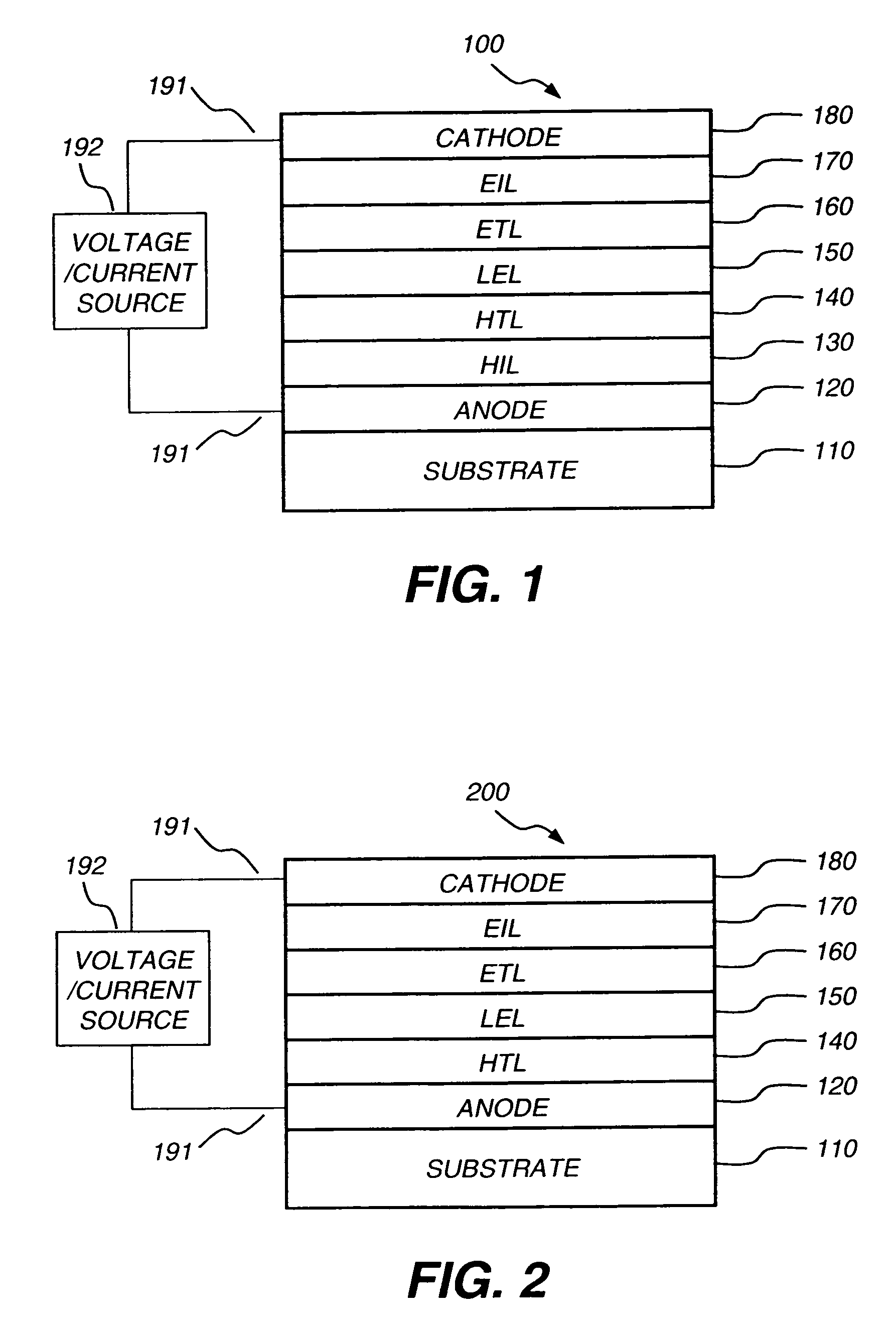
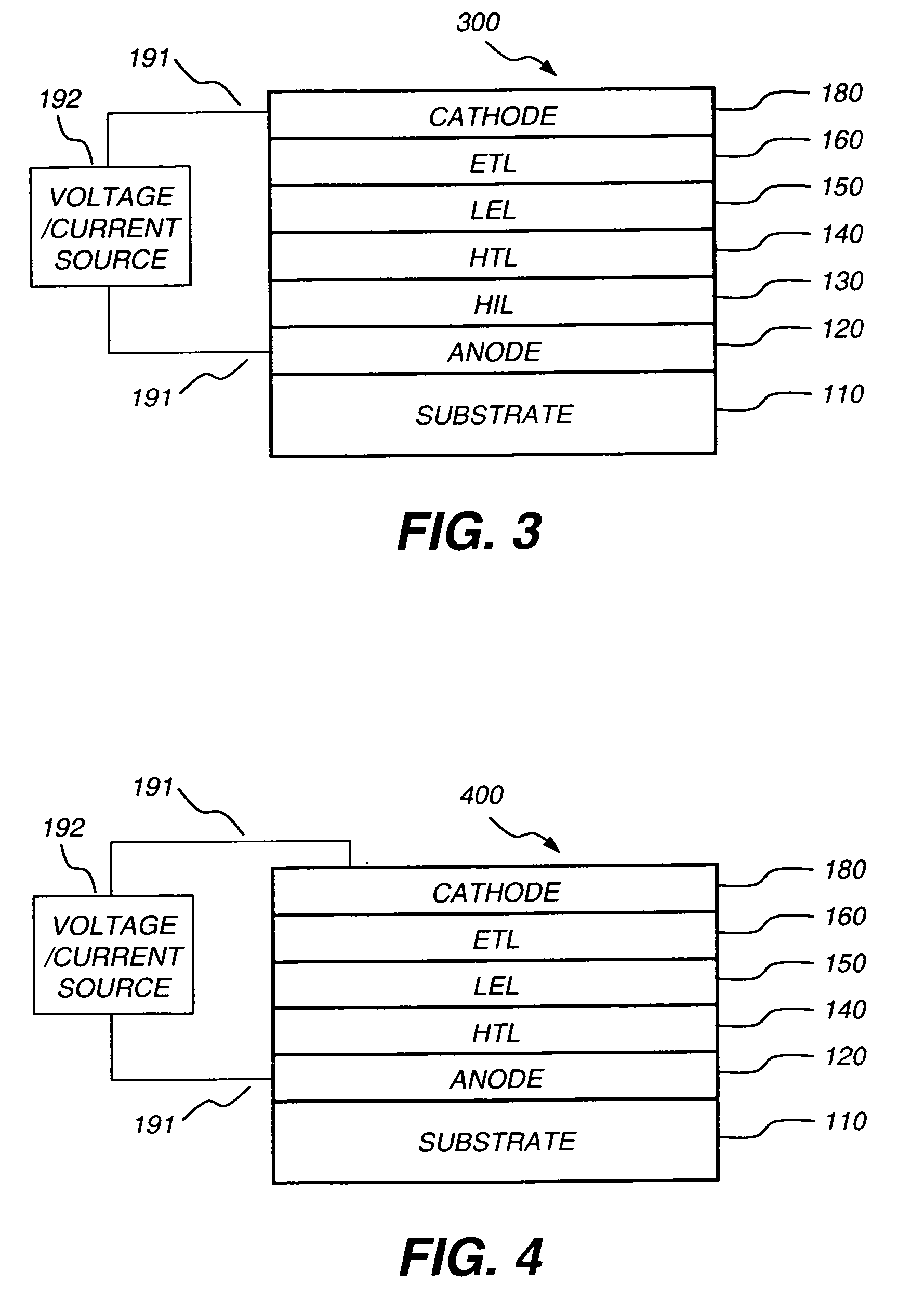
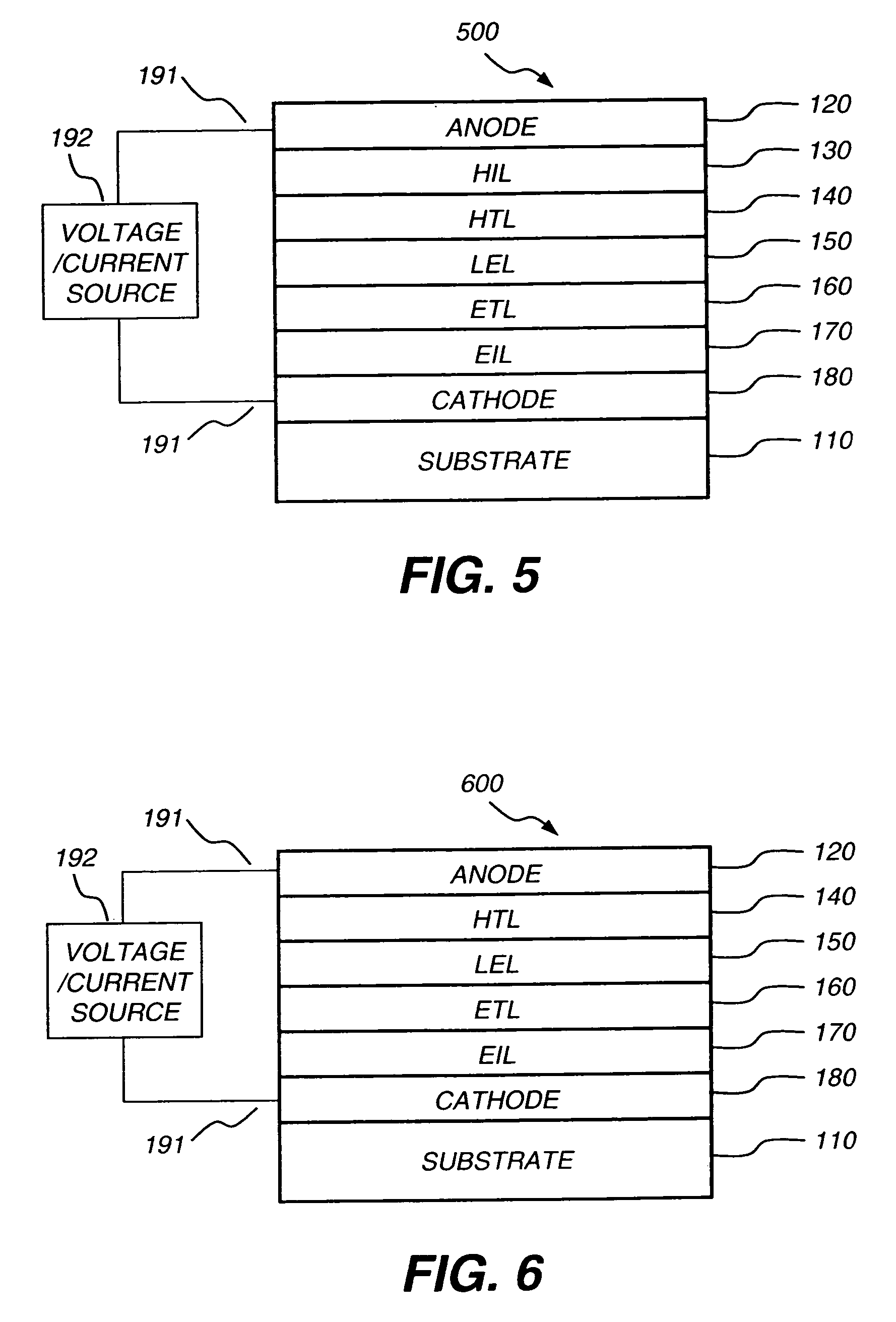
[0015] The present invention makes use of an ETL with an improved LEL / ETL interface both morphologically and electronically, having a material similar to the dominant host in the LEL but with a reduction potential greater than that of the dominant host in the LEL. It is an advantage of the present invention that the OLED, especially that with a blue color emission, containing this ETL has improved luminous efficiency, improved drive voltage, improved color gamut, and improved operational lifetime.
that the OLED, especially that with a blue color emission, containing this ETL has improved luminous efficiency, improved drive voltage, improved color gamut, and improved operational lifetime.

Problems solved by technology

However, when using this type of ETL in an OLED, the electron injection from the cathode into the LEL cannot be easy due to the lack of intermediate energy step between the Fermi level of the cathode and the LUMO (lowest unoccupied molecular orbital) of the LEL.
Therefore, in this case, the luminous efficiency of the OLED is not high enough and the drive voltage cannot be low enough for real applications.
For example, in a conventional blue OLED having TBADN as a dominant host in the LEL and having Alq as the material in the ETL, there is a relatively high electron injection barrier between the LUMO of Alq and that of TBADN at the LEL / ETL interface resulting in increased drive voltage.
In this case there is no hole-blocking effect because the HOMO of Alq is higher than that of TBADN causing low luminous efficiency.
However, because there is no similarity between the molecular structure of TBADN and Bphen, they are unlikely to form an effective interfacial contact.
This results in a fast deterioration of the interface, and thus the operational lifetime of the blue OLED having Bphen as ETL (or HBL) is dramatically short.

Method used


Image

  • OLED electron-transporting layer
  • OLED electron-transporting layer
  • OLED electron-transporting layer

Examples


example 4 (

Inventive)

[0207] An OLED, in accordance with the present invention, was constructed as the same as that in Example 3, except that the 5 nm thick ETL (layer c) includes Material F-3, instead of Alq.

[0208] This OLED requires a drive voltage of about 4.8 V to pass 20 mA / cm2. Under this test condition, the device has a luminance of 587 cd / m2, and a luminous efficiency of about 2.9 cd / A. Its color coordinates are CIEx=0.135 and CIEy=0.169, and its emission peak is at 461 nm. Its T80(70° C.@20 mA / cm2) is about 220 hours. The EL performance data are summarized in Table 1, and its normalized luminance vs. operational time, tested at 70° C. and at 20 mA / cm2, is shown in FIG. 9.

[0209] In this device, both the host material in the LEL and the material in the ETL are anthracene derivatives. The reduction potential of TBADN and F-3 were measured as about −1.90 V and −1.78 V vs. SCE in the 1:1 MeCN / toluene organic solvent system, respectively. Therefore, the reduction potential of F-3 is about ...

example 5 (

Inventive)

[0210] Another OLED, in accordance with the present invention, was constructed as the same as that in Example 3, except that the 5 nm thick ETL (layer c) includes Material F-3 doped with about 1.2 vol % lithium, instead of Alq.

[0211] This OLED requires a drive voltage of about 4.2 V to pass 20 mA / cm2. Under this test condition, the device has a luminance of 577 cd / m2, and a luminous efficiency of about 2.9 cd / A. Its color coordinates are CIEx=0.136 and CIEy=0.158, and its emission peak is at 460 nm. Its T80(70° C.@20 mA / cm 2) is projected as about 300 hours. The EL performance data are summarized in Table 1, its normalized luminance vs. operational time, tested at 70° C. and at 20 mA / cm2, is shown in FIG. 9, and its normalized EL spectrum is shown in FIG. 10.

[0212] In this device, both the host material in the LEL and the material in the ETL are anthracene derivatives. With lithium being incorporated in the ETL, the drive voltage, the operational stability, and the color...

example 6 (

Inventive)

[0213] An OLED, in accordance with the present invention, was constructed in the same manner as Example 3, except that the 5 nm thick ETL (layer c) includes Material G-1, instead of Alq.

[0214] This OLED requires a drive voltage of about 4.9 V to pass 20 mA / cm2. Under this test condition, the device has a luminance of 570 cd / m2, and a luminous efficiency of about 2.9 cd / A. Its color coordinates are CIEx=0.135 and CIEy=0.162, and its emission peak is at 462 nm. Its T80(70° C@20 mA / cm 2) is greater than 220 hours. The EL performance data are summarized in Table 1.

[0215] In this device, both the host material in the LEL and the material in the ETL are anthracene derivatives. The reduction potential of TBADN and G-1 were measured as about −1.90 V and −1.86 V vs. SCE in the 1:1 MeCN / toluene organic solvent system, respectively. Therefore, the reduction potential of G-1 is about 0.04 V greater than that of TBADN. Moreover, the oxidation potential of TBADN and G-1 were measured ...


PUM

PropertyMeasurementUnit
work functionaaaaaaaaaa
thicknessaaaaaaaaaa
HOMOaaaaaaaaaa

Abstract

An organic light-emitting device (OLED) includes an anode, a cathode, and a light-emitting layer disposed between the anode and the cathode, wherein the light-emitting layer includes a dominant host and a dopant. The device also includes an electron-transporting layer disposed in direct contact with the light-emitting layer on the cathode side, wherein the electron-transporting layer includes an electron-transporting material having the same chromophore as that of the dominant host in the light-emitting layer, wherein the electron-transporting material constitutes more than 50% by volume of the electron-transporting layer, and wherein the electron-transporting material has a greater reduction potential than that of the dominant host in the light-emitting layer.

Description

FIELD OF INVENTION [0001] This invention relates to organic light-emitting device (OLED). More specifically, this invention relates to OLED having an electron-transporting layer to improve the electroluminescence (EL) performance of the device. BACKGROUND OF THE INVENTION [0002] OLEDs, as described by Tang in commonly assigned U.S. Pat. No. 4,356,429, are commercially attractive because they offer the promise of low cost fabrication of high density pixel displays exhibiting bright EL with long lifetime, high luminous efficiency, low drive voltage, and wide color range. [0003] A typical OLED includes two electrodes and one organic EL unit disposed between the two electrodes. The organic EL unit commonly includes an organic hole-transporting layer (HTL), an organic light-emitting layer (LEL), and an organic electron-transporting layer (ETL). One of the electrodes is the anode, which is capable of injecting positive charges (holes) into the HTL of the EL unit. The other electrode is th...

Claims


Application Information

Patent Timeline
Patent Type & Authority Applications(United States)
IPC IPC(8): H01L51/54H05B33/12
CPCH01L51/0052H01L51/0054H01L51/0058H01L51/0059H01L51/0062H01L2251/308H01L51/0084H01L51/0085H01L51/0089H01L51/5048H01L51/5052H01L51/0081H10K85/649H10K85/622H10K85/615H10K85/631H10K85/626H10K85/341H10K85/351H10K85/324H10K85/342H10K50/165H10K50/14H10K2102/103
Inventor LIAO, LIANG-SHENGCONLEY, SCOTT R.COSIMBESCU, LELIAJARIKOV, VIKTOR V.
Owner EASTMAN KODAK CO
Why Eureka
Try Eureka