Oscillator coupling to reduce spurious signals in receiver circuits

a receiver circuit and oscillator technology, applied in the field of oscillators, can solve the problems of system damage, interference of the harmonics of buffered signals, etc., and achieve the effect of high input impedance and disabling the oscillator

Inactive Publication Date: 2006-11-30
ENTROPIC COMM INC
View PDF6 Cites 8 Cited by
  • Summary
  • Abstract
  • Description
  • Claims
  • Application Information

AI Technical Summary

Benefits of technology

[0007] The crystal oscillator of a first phase-locked loop (PLL) of a first receiver circuit is coupled to a second PLL of a second receiver. This crystal oscillator is shared between the two receiver circuits without using a buffered oscillator signal as in the prior art. By avoiding the use of the buffer, the detrimental harmonics caused by the buffer are eliminated. The reference input buffer of the second receiver circuit is specified according to the amplitude available from the crystal circuit, providing a moderately high input impedance. The extra load capacitance introduced by the device being driven and by the board trace is taken in account during the design of the crystal oscillator circuit. The crystal oscillator (XO) can be of any topology, for example a Pierce crystal oscillator.
[0008] In the invention, the crystal oscillator of the second slave receiver is disabled. The oscillator is disabled in the slave device to avoid having the amplified version of the input signal radiating on the board which may cause similar detrimental harmonics as would the use of an output buffer in the prior art. The disabling of the oscillator can be achieved by using one P-type field-effect transistor (FET) and one N-type FET to couple power to the amplifier used in the crystal oscillators.

Problems solved by technology

The harmonics of the buffered signal can be an interferer and detrimental to the system similar to unwanted signals picked up from the antenna.

Method used


Image

  • Oscillator coupling to reduce spurious signals in receiver circuits
  • Oscillator coupling to reduce spurious signals in receiver circuits
  • Oscillator coupling to reduce spurious signals in receiver circuits

Examples


Embodiment Construction

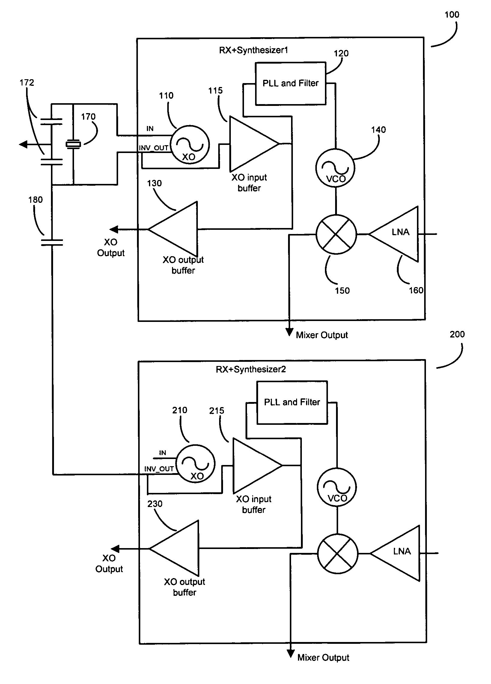
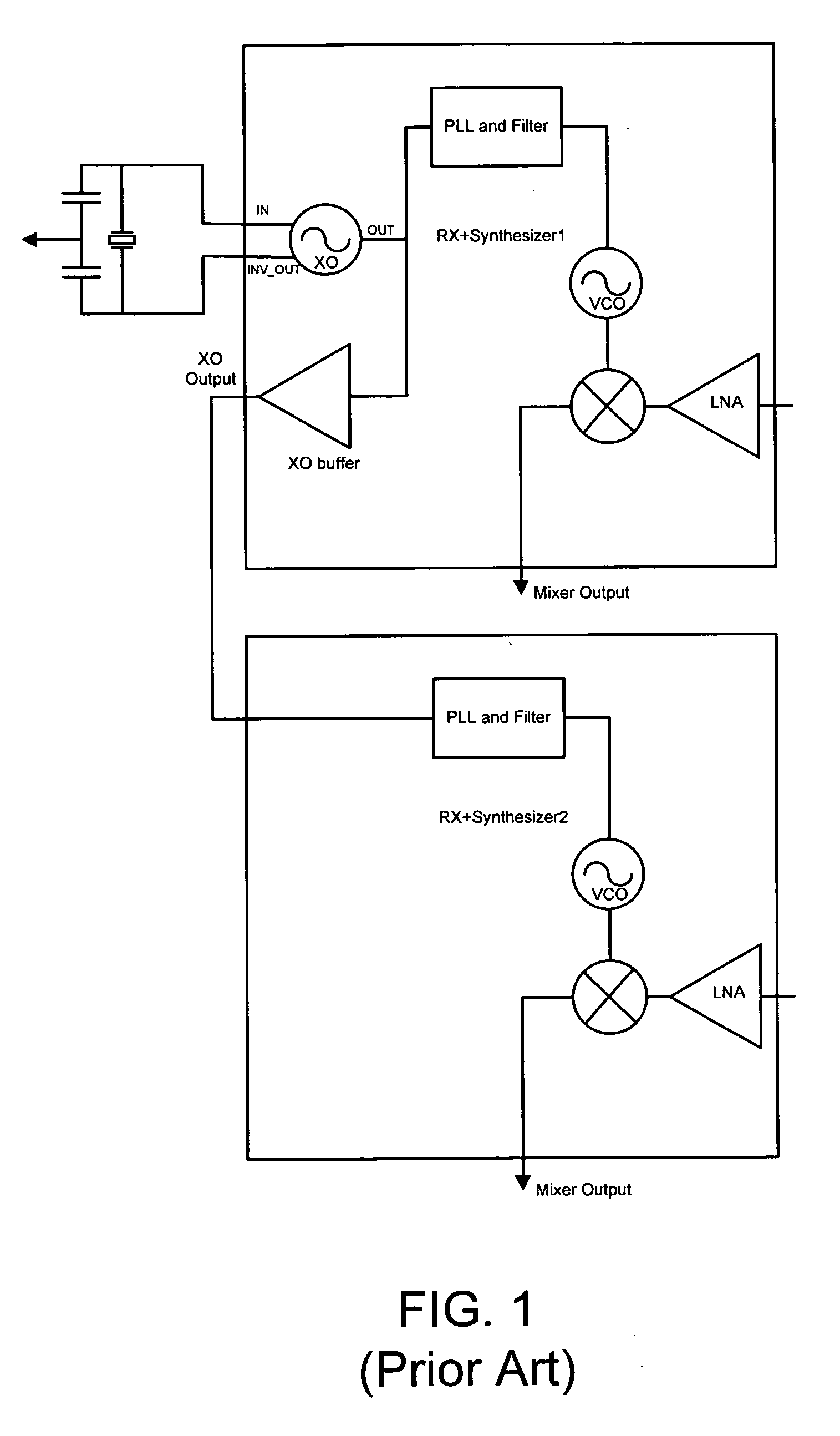
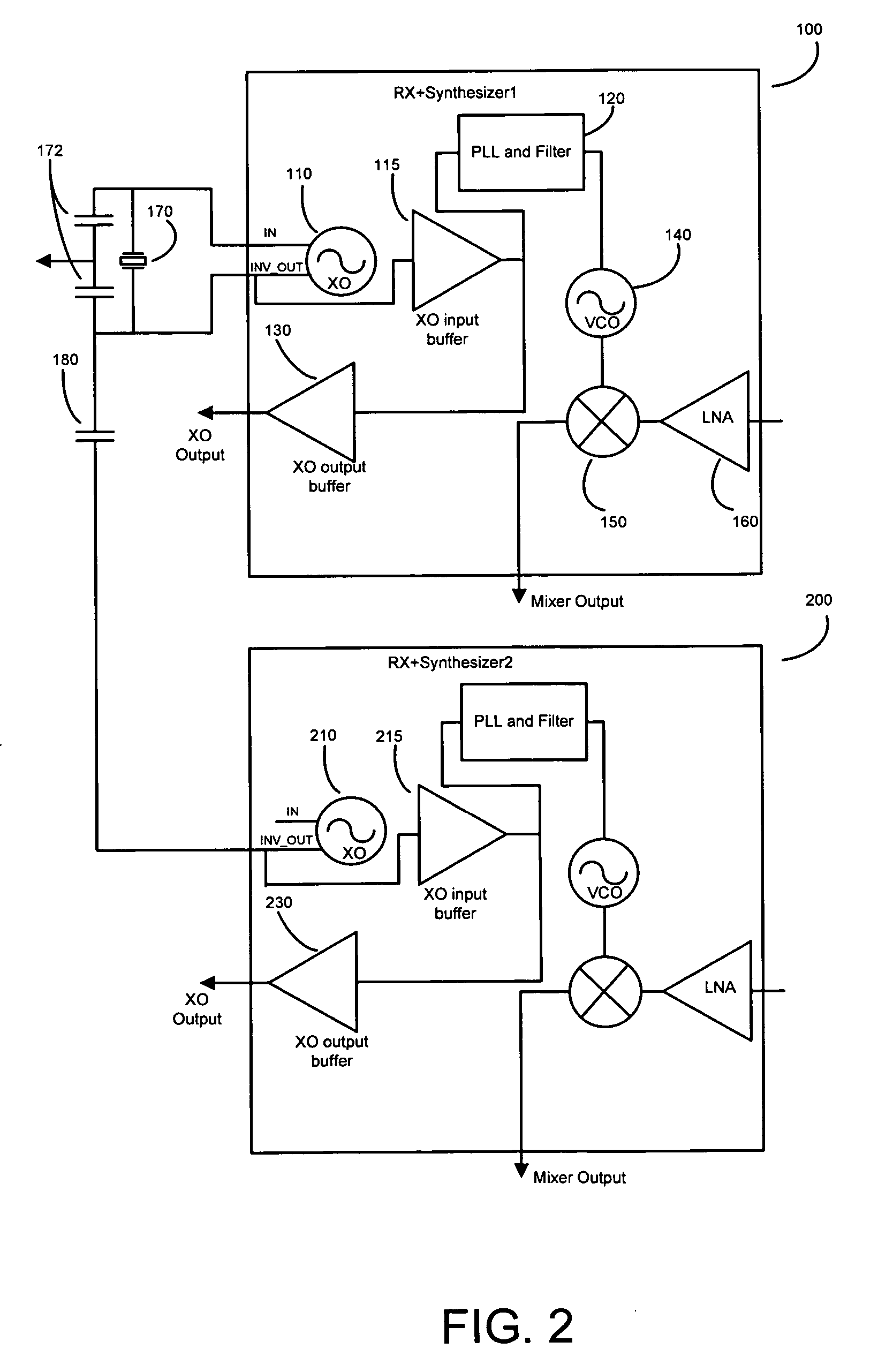
[0012]FIG. 2 shows a block diagram coupling an oscillator according to the present invention. Two receiver circuits are shown, master 100 and slave 200. Master 100 comprises crystal oscillator 110, phase-locked loop (PLL) and filter circuit 120, crystal oscillator (XO) input buffer 115, voltage controlled oscillator (VCO) 140, mixer 150 and low noise amplifier (LNA) 160. The crystal oscillator output buffer 130 would be used in the prior art method of coupling the oscillator signal to a second receiver. Capacitors 172 provide the capacitance to achieve the necessary requirement that the overall loop gain has zero (or 360) degrees phase shift at the oscillation frequency. The crystal 170 is connected such that it forms part of the feedback impedance of the inverting amplifier in the crystal oscillator circuit 110, which operates in a non-saturating linear or near linear mode.

[0013] Oscillator 110 drives receiver 200 through capacitor 180, which isolates the direct current bias of os...


PUM


Abstract

A first receiver frequency reference is passively coupled to a second receiver by tapping a signal directly from the resonant element, such as a crystal, of an oscillator in the first receiver to drive the input of the second receiver. The sinusoidal signal from the resonant element is relatively free of harmonics and minimizes interference that could be caused by harmonics of a square wave signal coupling or an amplified signal. The oscillator of each receiver can be selectively enabled or disabled to allow the receiver to either generate or receive the frequency reference. This technique of coupling can be used to couple a frequency reference signal between integrated circuit receivers.

Description

RELATED APPLICATIONS [0001] This application claims priority from U.S. provisional application No. 60 / 684,505 filed May 25, 2005 entitled “Method of coupling oscillators to reduce spurious signals in receiver circuits”, incorporated herein by reference.BACKGROUND [0002] 1. Field of the Invention [0003] The present invention relates to oscillators and specifically to coupling a common reference between two oscillator circuits. [0004] 2. Prior Art [0005] In receiver circuits, it is common practice to buffer the crystal oscillator signal of a phase-locked loop (PLL) of a first receiver circuit and use the buffered version of the signal as the reference for the phase-locked loop (PLL) of a second receiver circuit. The buffer used is commonly a saturated amplifier with its output signal being almost a square wave. This square wave output has a high number of harmonics present and some of these harmonics can end up present in the band of the receiver or the band of the mixer's output. The...

Claims


Application Information

Patent Timeline
Patent Type & Authority Applications(United States)
IPC IPC(8): H04B7/00
CPCH04B1/403H04B1/28
Inventor BISANTI, BIAGIOCOPPOLA, FRANCESCOCIPRIANI, STEFANO
Owner ENTROPIC COMM INC
Why Eureka
Try Eureka