Semiconductor device having SiC substrate and method for manufacturing the same

a technology of semiconductor devices and substrates, which is applied in the direction of semiconductor/solid-state device manufacturing, semiconductor devices, electrical devices, etc., can solve the problems of damage to the reaction layer, difficult to completely remove the intermediate product layer b>3/b>, etc., and achieve excellent ohmic contact, excellent ohmic contact, and high-quality surface metallization

Inactive Publication Date: 2006-12-07
DENSO CORP +1
View PDF6 Cites 68 Cited by
  • Summary
  • Abstract
  • Description
  • Claims
  • Application Information

AI Technical Summary

Benefits of technology

[0011] In the above device, the silicide layer provides excellent ohmic contact with the SiC substrate. The carbide layer functions as a stopper layer for preventing a carbon atom from diffusing and exposing on the surface of the substrate. Thus, a carbon related particle and a carbon particle do not exposed on the surface of the carbide layer. Accordingly, an electrode and a wiring to be formed on the carbide layer is prevented from peeling off from the carbide layer. Further, there is no need to remove the carbon related particle and the carbon particle from the surface of the carbide layer. Accordingly, the silicide layer and the carbide layer have no damage caused by removal step, so that the ohmic contact is sufficiently secured. Thus, the device has excellent ohmic contact and a high quality surface metallization construction having no damage.
[0013] The above method provides the device having excellent ohmic contact. Further, an electrode and a wiring to be formed on the carbide layer is prevented from peeling off from the carbide layer. Furthermore, the silicide layer and the carbide layer have no damage caused by removal step, so that the ohmic contact is sufficiently secured. Thus, the device has excellent ohmic contact and a high quality surface metallization construction having no damage.

Problems solved by technology

Therefore, even when the physical method is performed to remove the intermediate product layer 3, it is difficult to remove the intermediate product layer 3 completely.
Further, removal of the intermediate product layer 3 by means of the physical method may damage the reaction layer 2a.

Method used


Image

  • Semiconductor device having SiC substrate and method for manufacturing the same
  • Semiconductor device having SiC substrate and method for manufacturing the same
  • Semiconductor device having SiC substrate and method for manufacturing the same

Examples


Embodiment Construction

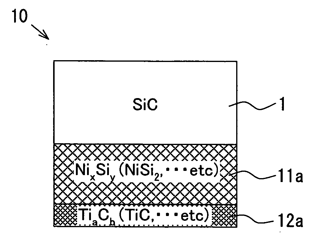
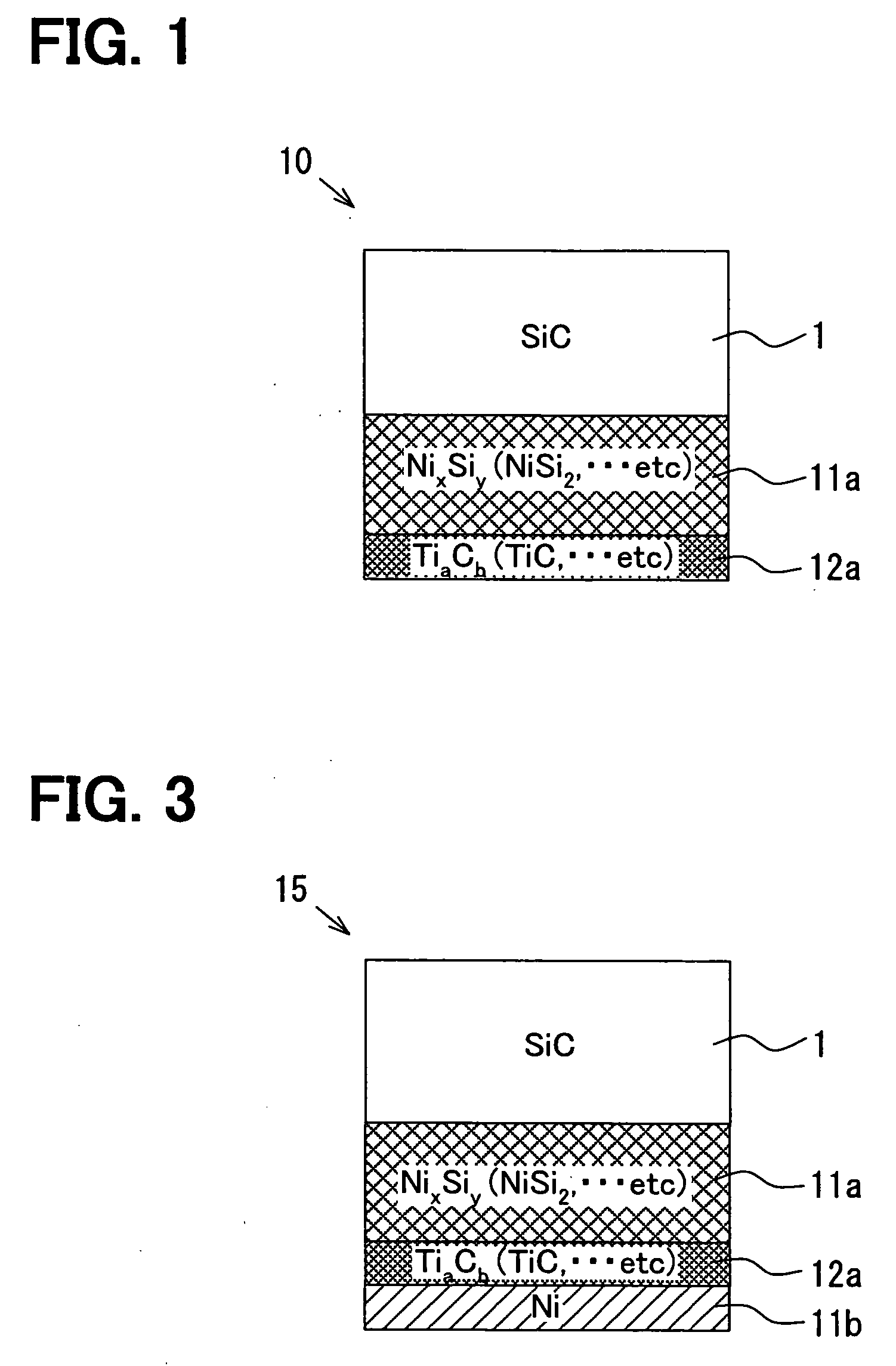
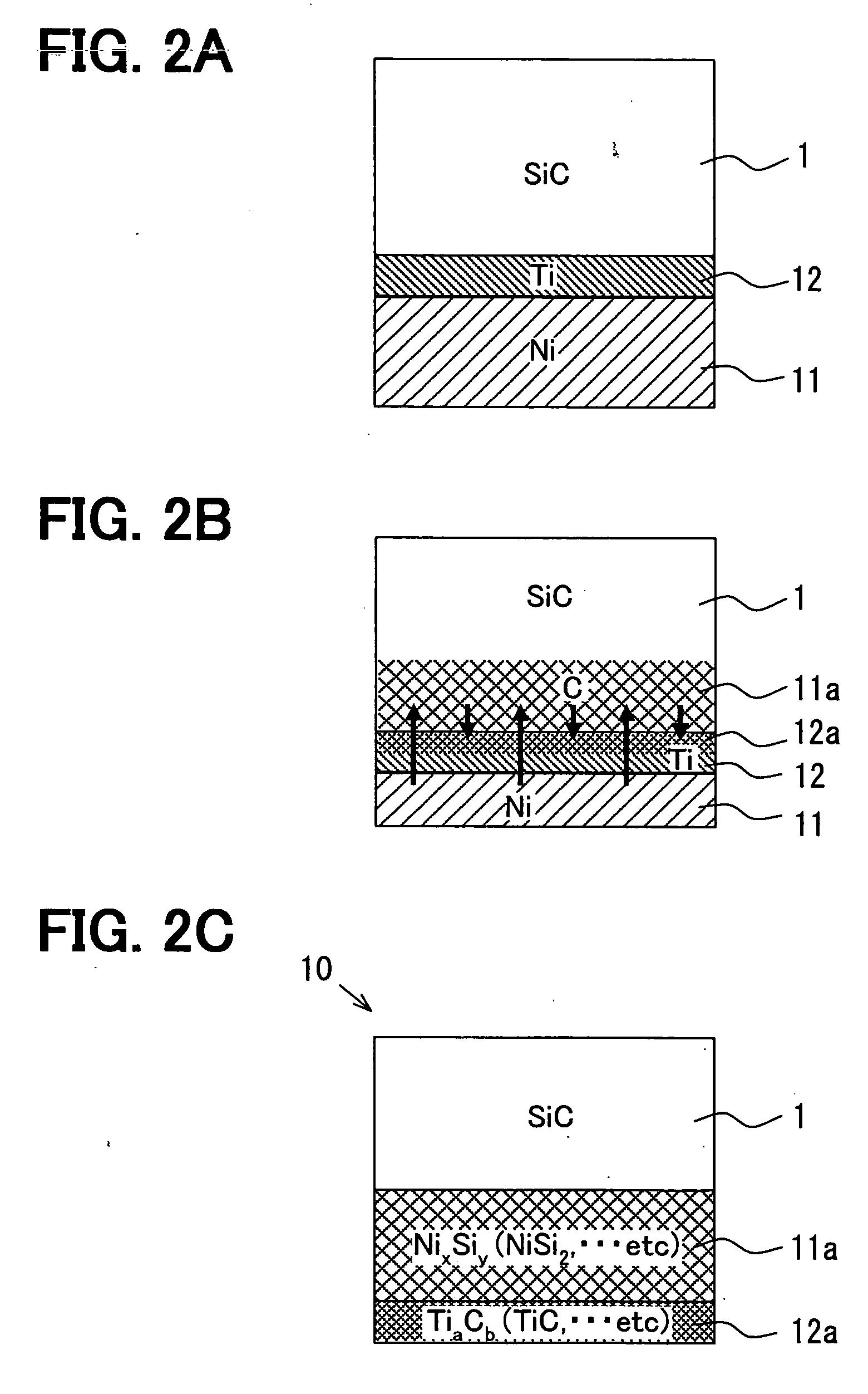
[0022] A SiC semiconductor device having a SiC substrate according to a preferred embodiment is described. The device further includes a first metallic layer and a second metallic layer, which are disposed on the surface of the SiC substrate in this order. The first metallic layer is made of silicide including nickel (i.e., Ni) or nickel alloy. The second metallic layer is made of carbide including titanium (i.e., Ti), tantalum (i.e. Ta) or tungsten (i.e., W).

[0023]FIG. 1 shows an example of a semiconductor device according to the preferred embodiment. The semiconductor device 10 includes a SiC substrate 1. On the surface of the SiC substrate 1, a silicide layer 11a as the first metallic layer including nickel di-silicide (i.e., NiSi2) or the like and a carbide layer 12a as the second metallic layer including titanium carbide (i.e., TiC) are formed in this order. The silicide layer 11a is made from NixSiy. For example, the silicide layer 11a is a NiSi2 layer. The carbide layer 12a ...


PUM

PropertyMeasurementUnit
thicknessaaaaaaaaaa
thicknessaaaaaaaaaa
temperatureaaaaaaaaaa

Abstract

A semiconductor device includes: a SiC substrate; a silicide layer disposed on the SiC substrate; and a carbide layer disposed on the silicide layer. The silicide layer includes a first metal, and the carbide layer includes a second metal. The first metal is Ni or Ni alloy, and the second metal is Ti, Ta or W. The device provides excellent ohmic contact and high quality surface metallization construction.

Description

CROSS REFERENCE TO RELATED APPLICATION [0001] This application is based on Japanese Patent Application No. 2005-167401 filed on Jun. 7, 2005, the disclosure of which is incorporated herein by reference. FIELD OF THE INVENTION [0002] The present invention relates to a semiconductor device having a SiC substrate and a method for manufacturing the same. BACKGROUND OF THE INVENTION [0003] A semiconductor device having a SiC substrate is disclosed in, for example, Japanese Patent Application Publication No. 2003-243323. Specifically, an electrode construction of the device and a method for manufacturing the device are disclosed. [0004]FIGS. 7A to 7D shows a method for manufacturing a semiconductor device having a SiC substrate according to a comparison of an embodiment of the present invention. Specifically, the method shown in FIGS. 7A to 7D is a surface metallization method, which is suitably used for forming an electrode. A metallization layer is formed on a backside of the SiC substr...

Claims


Application Information

Patent Timeline
Patent Type & Authority Applications(United States)
IPC IPC(8): H01L31/0312
CPCH01L29/1608H01L21/0485
Inventor YAMAMOTO, TAKEOKUMAR, MALHAN RAJESHTAKEUCHI, YUUICHIVASSILEVSKI, KONSTANTINWRIGHT, NICHOLAS
Owner DENSO CORP
Why Eureka
Try Eureka