Method of fabricating periodic nano-structure arrays with different feature sizes

a technology of feature size and nano-structure array, which is applied in the direction of instruments, electrical equipment, nanotechnology, etc., can solve the problems of loss of resolution, time-consuming and relatively expensive process, and the density of the overall device, so as to achieve less expensive and maintain the resolution of the device

Inactive Publication Date: 2006-12-07
AGENCY FOR SCI TECH & RES
View PDF10 Cites 12 Cited by
  • Summary
  • Abstract
  • Description
  • Claims
  • Application Information

AI Technical Summary

Benefits of technology

[0006] It is therefore an object of the present invention to provide a method of fabricating an array of features on a substrate using a method that is less expensive than methods of the prior art whilst maintaining resolution of the device.

Problems solved by technology

Customizing the fabrication process to include regions of features of varying size is a time consuming and relatively expensive process compared to the fabrication of a device having uniform features.
However, this may affect the density of the overall device and so lead to a loss of resolution.

Method used


Image

  • Method of fabricating periodic nano-structure arrays with different feature sizes
  • Method of fabricating periodic nano-structure arrays with different feature sizes
  • Method of fabricating periodic nano-structure arrays with different feature sizes

Examples


Embodiment Construction

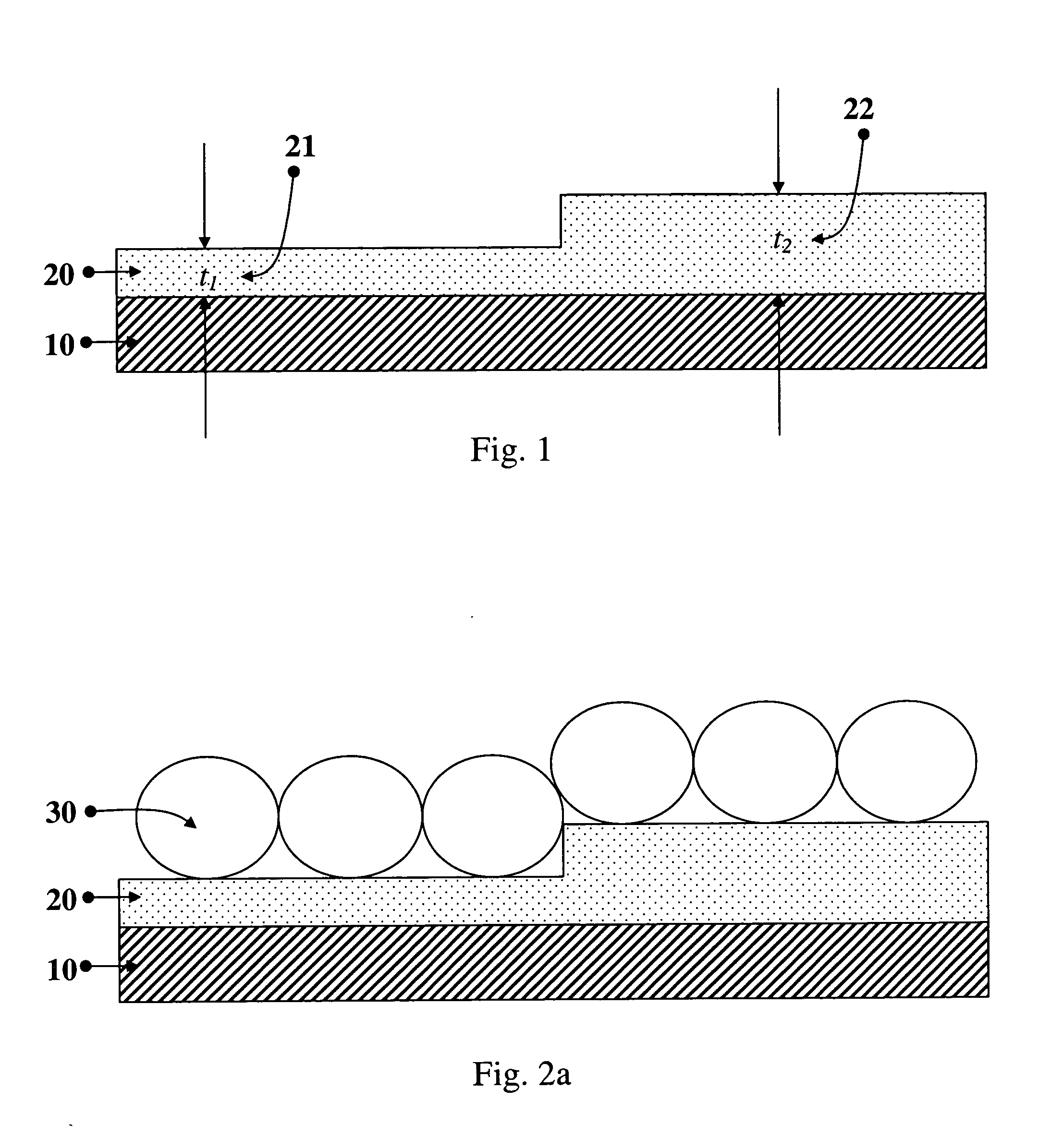
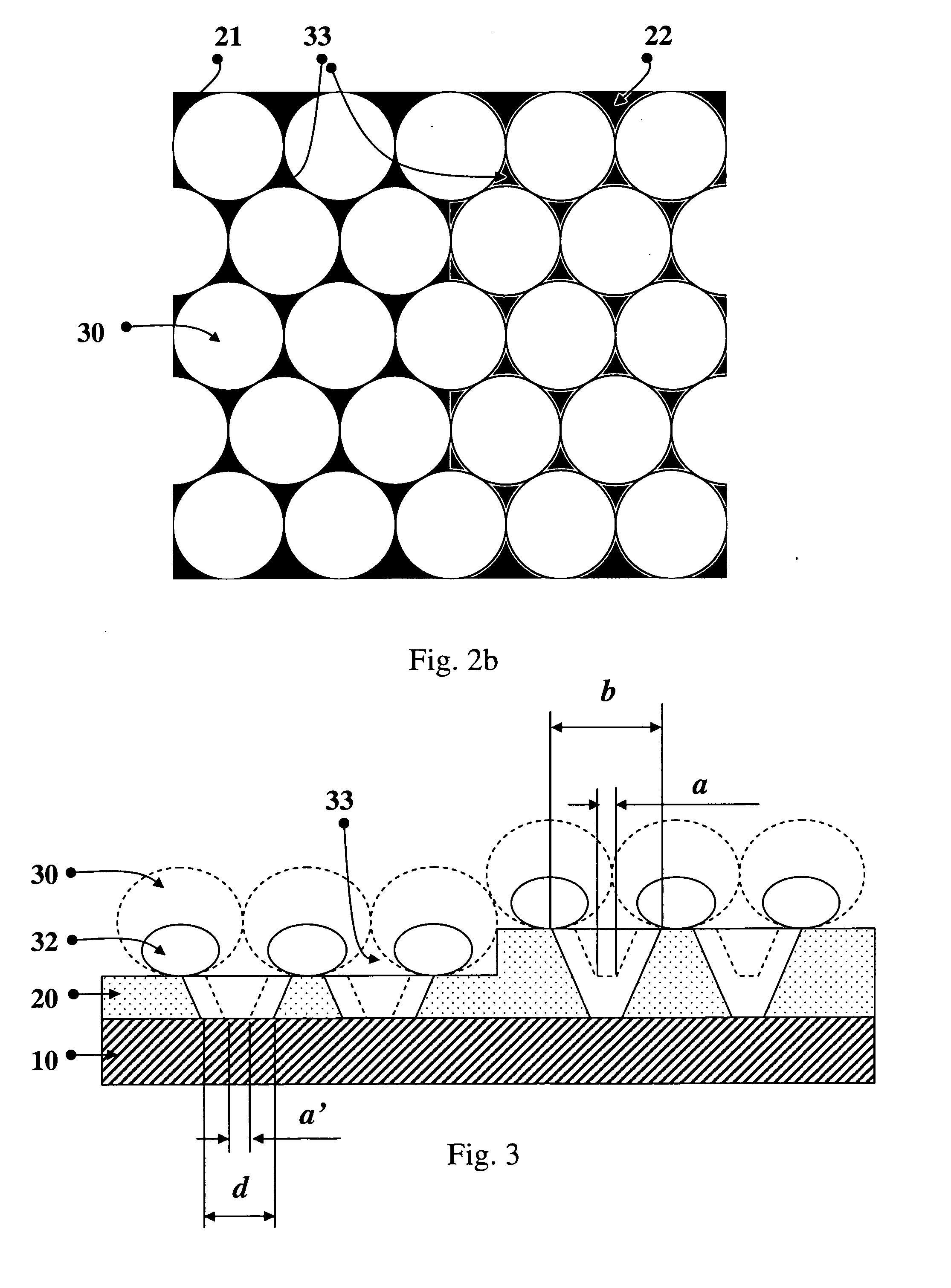
[0027] The present invention seeks to provide a simple and fast method for fabricating multi-sized patterned arrays and nano-meter scale structured arrays having different sizes deposited through the patterned arrays. These different sized arrays may be used in fabricating semiconductor light sources having different emitting wavelengths, or fabricating semiconductor photodetectors having different response wavelength, or fabricating 2D photonic crystal materials having different properties

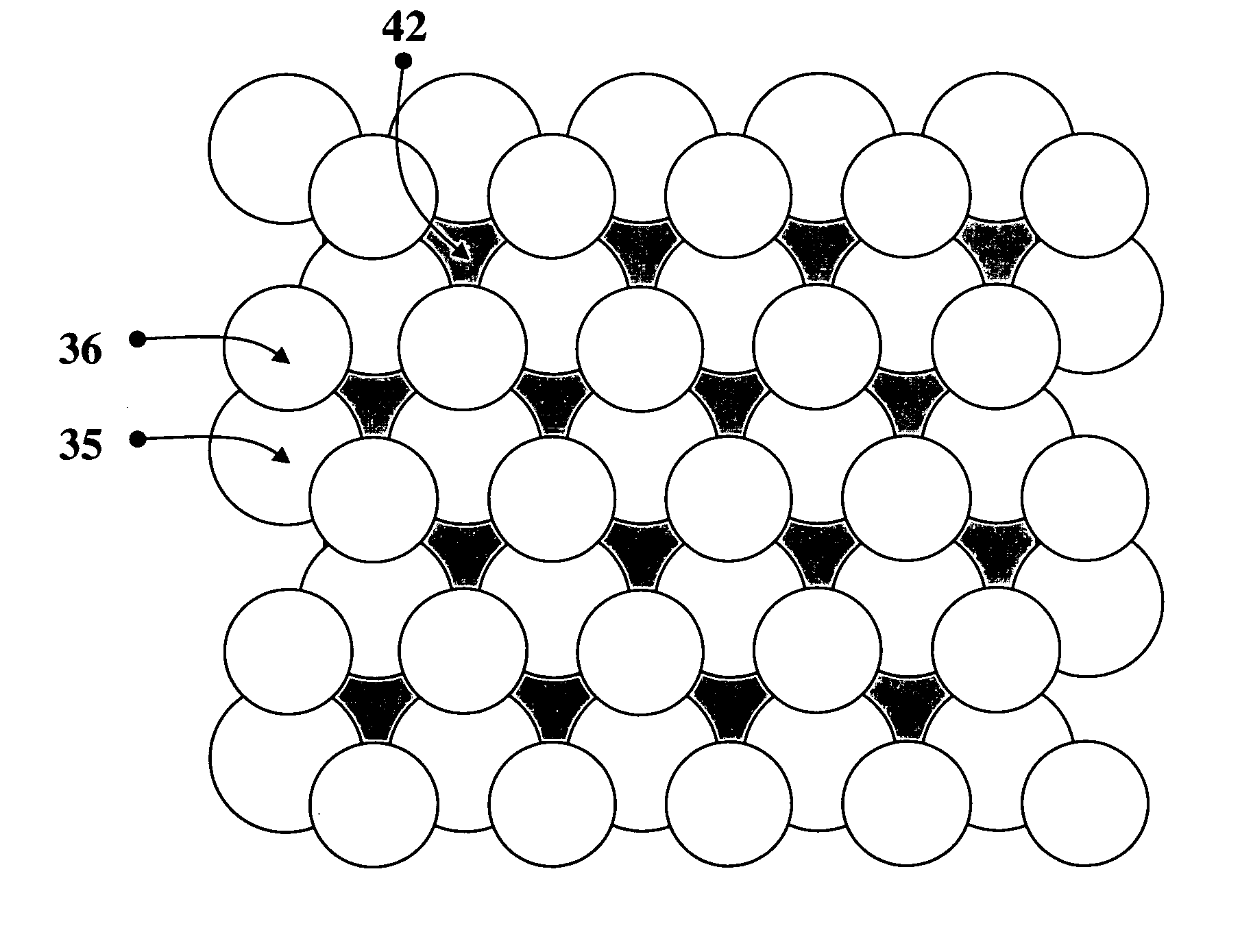
[0028] In the present invention, a method is provided for nano-meter scaled pattern formation on a selected substrate. This process opens a route for nano-meter scale surface patterning by utilizing spontaneous self-assembly of latex spheres at length scales difficult to obtain by standard semiconductor lithography techniques. This method also provides an easy, inexpensive, and fast means for pattern transfer over large areas.

[0029] The method is based on the principle that elements, for instanc...


PUM


Abstract

A method of fabricating a two dimensional nano-structure array of features comprising the steps of providing a substrate (10); forming an intermediate layer on said substrate (20), said intermediate layer having at least two selectively located regions (21, 22) of different uniform thickness; placing at least one layer of elements (30) over said intermediate layer, said elements placed in a close-packed arrangement forming an array of voids (33) between said elements; etching the intermediate layer through said voids, and so forming the array of features (51, 52) in said intermediate layer corresponding to the voids.

Description

CROSS-REFERENCE TO RELATED APPLICATIONS [0001] This application claims priority from U.S. Provisional Patent Application No. 60 / 663,084, filed on Mar. 17, 2005, which is incorporated herein by reference in its entirety.FIELD OF THE INVENTION [0002] The invention relates to the fabrication of nano-scale devices on a substrate. Specifically the invention relates to a method of fabricating arrays of different size features leading to the formation of devices of different sizes on the same substrate. BACKGROUND [0003] The fabrication of nano-scale optical devices requires the formation of arrays of individual features representing light sources or photo detectors within such devices. It follows that the density of such features will determine the sensitivity of the device and so requiring the mass scale fabrication of said features in order to improve performance. [0004] However, to increase flexibility and broaden the application of use, such devices require the fabrication of differen...

Claims


Application Information

Patent Timeline
Patent Type & Authority Applications(United States)
IPC IPC(8): H01L21/00
CPCG02B1/00B82Y20/00
Inventor WANG, BENZHONGCHUA, SOO JIN
Owner AGENCY FOR SCI TECH & RES
Why Eureka
Try Eureka