Analog-to-digital conversion circuit and image processing circuit for stepwise conversion of a signal through multiple stages of conversion units

an image processing circuit and digital conversion technology, applied in analogue/digital conversion, power saving provisions, instruments, etc., can solve the problems of deterioration in characteristics, increase in size, and decrease in conversion accuracy, so as to avoid deterioration in characteristics, reduce power consumption, and reduce the effect of power consumption

Active Publication Date: 2005-04-19
SEMICON COMPONENTS IND LLC
View PDF8 Cites 6 Cited by
  • Summary
  • Abstract
  • Description
  • Claims
  • Application Information

AI Technical Summary

Benefits of technology

[0007]The present invention has beer, achieved in view of the foregoing circumstances. It is therefore an object of the present invention to provide an AD converter which operates with lower power consumption. It is another object of the invention to provide an AD conve

Problems solved by technology

Reducing the overall voltage range for an analog signal to realize lower power consumption would readily cause degradation in conversion accuracy clue to decreases in S/N ratio.
Th

Method used


Image

  • Analog-to-digital conversion circuit and image processing circuit for stepwise conversion of a signal through multiple stages of conversion units
  • Analog-to-digital conversion circuit and image processing circuit for stepwise conversion of a signal through multiple stages of conversion units
  • Analog-to-digital conversion circuit and image processing circuit for stepwise conversion of a signal through multiple stages of conversion units

Examples


first embodiment

(First Embodiment)

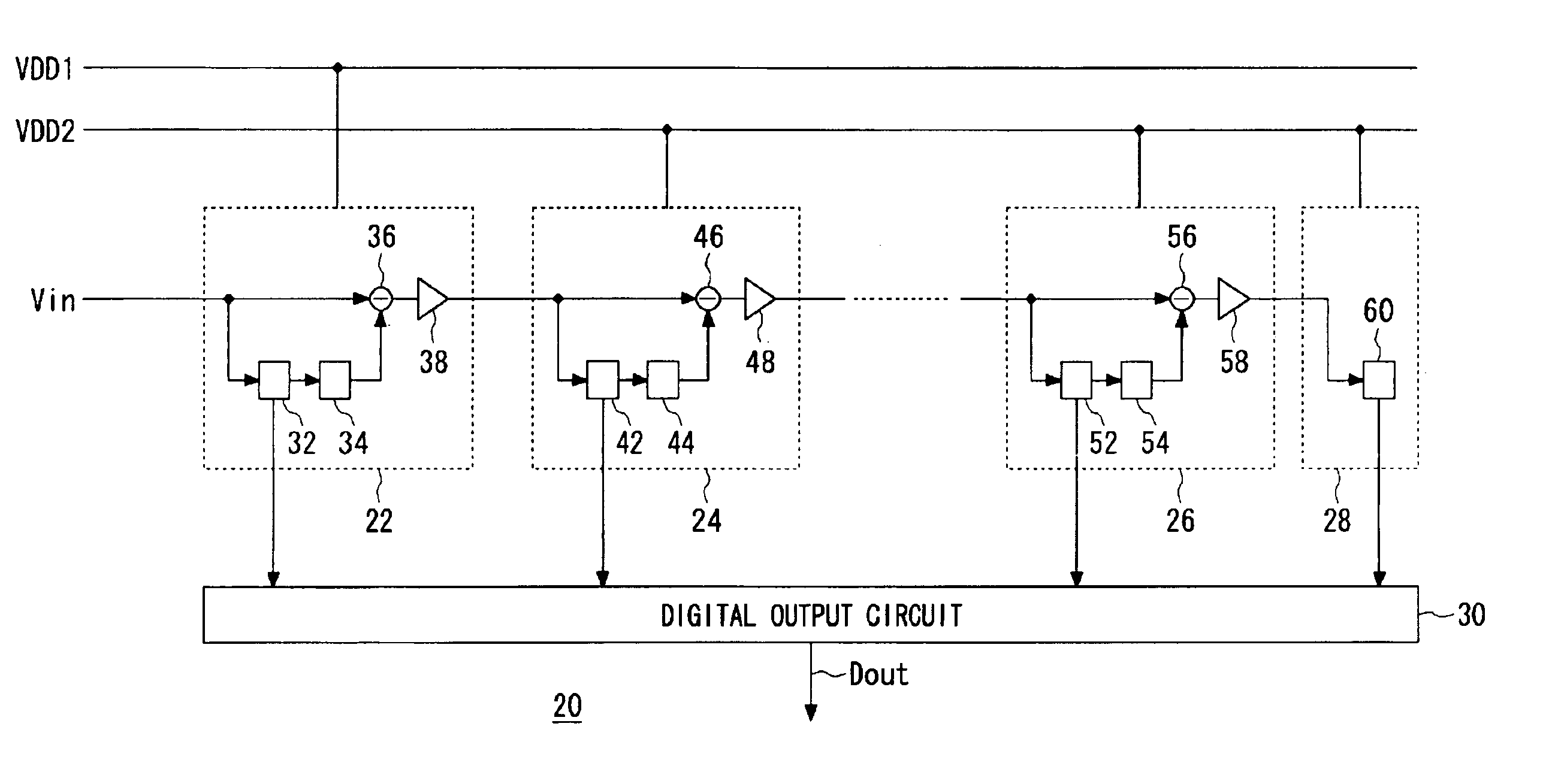
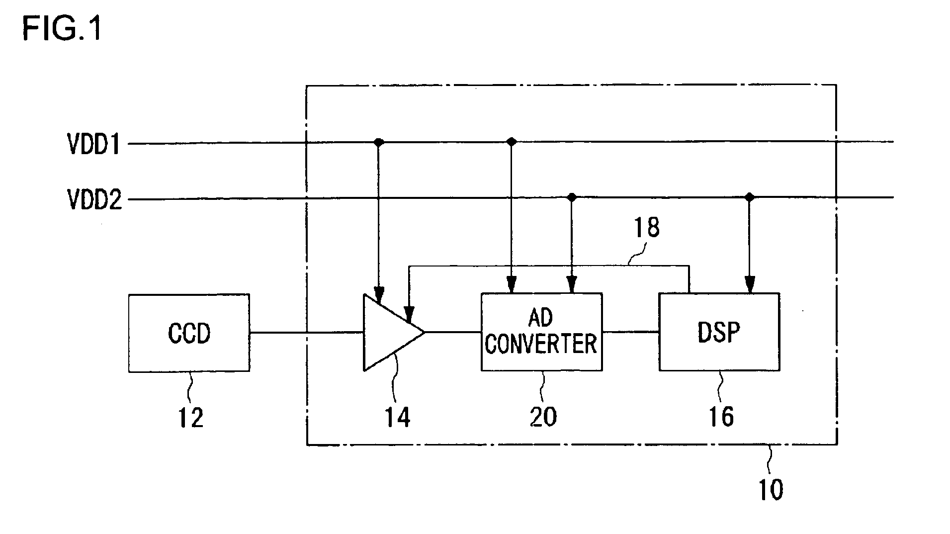
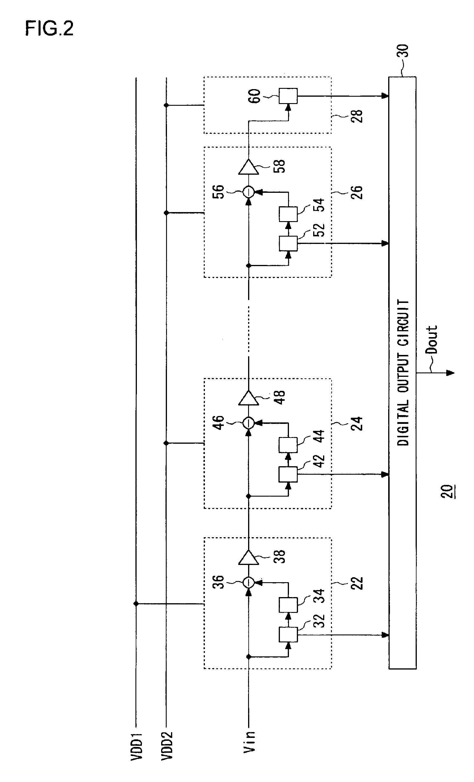
[0022]FIG. 1 shows the basic configuration of an image processing circuit. An image sensor 12 such as CCD (Charge Coupled Device) and a CMOS sensor receives light from a subject to convert the light into an electric signal, which is then supplied to a one-chip LSI (Large Scale Integration) 10. The one-chip LSI 10 incorporates an AGC (Auto Gain Control) 14, an AD converter 20, and a DSP (Digital Signal Processor) 16. The AGC 14 amplifies the electric signal received from the image sensor 12, and the AD converter 20 converts the amplified analog signal into a digital signal, on which the DSP 16 performs compression or other image processing. Part of the output from the DSP 16 is fed back to the AGC 14 via a feedback circuit 18.

[0023]The one-chip LSI 10 is supplied with power from two sources, i.e., a first voltage source VDD1 and a second voltage source VDD2. The first voltage source VDD1 supplies 2.7V and the second voltage source VDD2 supplies 1.2V. Thus, the AGC 1...

second embodiment

(Second Embodiment)

[0031]FIG. 3 shows the configuration of an AD converter 20 according to a second embodiment. The AD converter 20 according to this embodiment is different from that of the first embodiment in that voltages to be supplied to each of multiple stages of conversion units are gradually lowered. Now, the different point will be mainly described below.

[0032]The first conversion unit 22 and the second conversion unit 24 are supplied with a voltage from the first voltage source VDD1 and a voltage from the second voltage source VDD2, respectively. On the other hand, the (n−1)th conversion unit 26 and the nth conversion unit 28 are supplied with a voltage from a third voltage source VDD3 and a voltage from a fourth voltage source VDD4, respectively. The first voltage source VDD1 supplies the highest voltage, while the second voltage source VDD2 supplies the second highest voltage, the third voltage source VDD3 the third highest voltage, and the fourth voltage source VDD4 the...

third embodiment

(Third Embodiment)

[0033]FIG. 4 shows the configuration of an AD converter 20 according to a third embodiment. The AD converter 20 according to this embodiment is different from that of the first and second embodiments in that the second voltage source VDD2 supplies a voltage to all of multiple stages of conversion units. Now, the different point will be mainly described below.

[0034]The AD converter 20 has a voltage step-up unit 82 for stepping up the voltage supplied. The step-up unit 82 steps up the voltage, supplied by the second voltage source VDD2 to the first conversion unit 22, from 1.2V to 2.7V. For example, the step-up unit 82 includes a charge pumping DC-DC converter. In this manner, a higher voltage is supplied only to the first stage or the first conversion unit 22, while a lower voltage is supplied to the second and subsequent stages or the second conversion unit 24 to the nth conversion unit 28, thereby reducing the overall voltage. Correspondingly, as in the first embo...


PUM


Abstract

A multi-stage pipelined AD converter has n stages of conversion units, such as a first conversion unit, a second conversion unit, an (n−1)th conversion unit, and an nth conversion unit, which successively convert an analog signal into a digital signal each by several bits starting from the most significant bit. Each of the converted digital signals of several bits is combined in a digital output circuit. A first voltage source supplies a higher voltage than a second voltage source. The first voltage source supplies a high voltage to the first stage or the first conversion unit, while the second voltage source supplies a low voltage to the second and subsequent stages of the second conversion unit to the nth conversion unit which require a lower analog accuracy.

Description

BACKGROUND OF THE INVENTION[0001]1. Field of the Invention[0002]The present invention relates to an analog-to-digital conversion circuit, and more particularly to a technique for reducing power consumption in the analog-to-digital conversion circuit.[0003]2. Description of the Related Art[0004]Recently, cellular phones have been provided with various additional functions such as an image shooting function, an image reproducing function, a moving image shooting function, and a moving image reproducing function. Accordingly, there are increasing needs for an analog-to-digital converter (hereinafter referred to as an “AD converter”) incorporated into the cellular phone to operate at lower voltages with lower power consumption. In particular, one-chip LSIs incorporating an AD converter has employed finer design rules year by year, and thus required lower supply voltages. As an AD converter having high conversion accuracy, known to those skilled in the art is a multi-stage pipelined AD c...

Claims


Application Information

Patent Timeline
IPC IPC(8): H03M1/14H03M1/38H03M1/12H03M1/44H03M1/60H03M1/46H03M1/00H03M1/16
CPCH03M1/002H03M1/167
Inventor WADA, ATSUSHITANI, KUNIYUKI
Owner SEMICON COMPONENTS IND LLC
Why Eureka
Try Eureka