Semiconductor memory device, semiconductor device, and method for production thereof

a semiconductor and memory device technology, applied in the direction of semiconductor devices, electrical devices, transistors, etc., can solve the problems of difficult to reduce the area of cell arrays, and achieve the effect of reducing size, reducing area, and reducing area

Inactive Publication Date: 2006-12-07
SONY CORP
View PDF4 Cites 8 Cited by
  • Summary
  • Abstract
  • Description
  • Claims
  • Application Information

AI Technical Summary

Benefits of technology

[0058] The semiconductor memory device according to the present invention is characterized in that the memory node contact plug and the semiconductor layer are connected to each other through a metallized region in place of impurity diffused from the memory node contact plug. This structure eliminates heat treatment for impurity diffusion from the memory node contact plug, and hence no distance is necessary for alignment of lithography to make the contact hole with lithography to form the gate electrode. This leads to a cell array with a reduced area.
[0059] The semiconductor device according to the present invention is characterized in that the contact plug and the semiconductor layer are connected to each other through a metallized region in place of impurity diffused from the contact plug. This structure eliminates heat treatment for impurity diffusion from the contact plug, and hence no distance is necessary for alignment for impurity diffusion. This leads to a semiconductor device with a reduced size.
[0060] The method for production of a semiconductor memory device according to the present invention is characterized in that the memory node contact plug is connected to the semiconductor layer through a metallized region. This method eliminates heat treatment for impurity diffusion from the memory node contact plug, and hence no distance is necessary for alignment of lithography to make the contact hole with lithography to form the gate electrode. This leads to a cell array with a reduced area.
[0061] The method for production of a semiconductor device according to the present invention is characterized in that the contact plug and the semiconductor layer are connected to each other through a metallized region. This method eliminates heat treatment for impurity diffusion from the contact plug, and hence no distance is necessary for alignment for impurity diffusion. This leads to a semiconductor device with a reduced size.

Problems solved by technology

The problem is that a certain distance is necessary for alignment of lithography to make the contact hole (for memory node contact) with lithography to form the gate electrode.
This makes it difficult to reduce the cell array area.

Method used


Image

  • Semiconductor memory device, semiconductor device, and method for production thereof
  • Semiconductor memory device, semiconductor device, and method for production thereof
  • Semiconductor memory device, semiconductor device, and method for production thereof

Examples


first embodiment

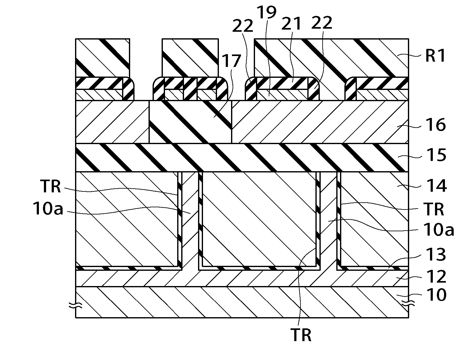
[0079]FIG. 1 is a sectional view of the memory cell of the DRAM pertaining to the present invention.

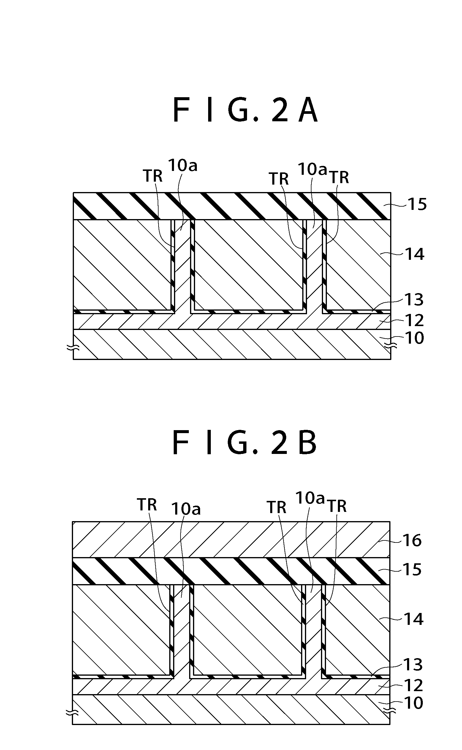
[0080] There is shown a semiconductor substrate 10, in which is a trench TR separated by a trench wall 10a. There is shown a first n-type semiconductor layer 12 with a prescribed depth from the surface of the inner wall of the trench TR. It functions as a plate electrode PL of the memory capacitor.

[0081] There is shown a capacitor insulating film 13 which covers the surface of the inner wall of the trench TR. There is shown a second n-type semiconductor layer 14 of polysilicon which fills the inside of the capacitor insulating film 13. It functions as the memory node electrode MN of the memory capacitor.

[0082] As mentioned above, the memory capacitor is composed of the first n-type semiconductor layer 12 (plate electrode PL), the capacitor insulating film 13, and the second n-type semiconductor layer 14 (memory node electrode MN).

[0083] There is shown an interlayer insulating film...

second embodiment

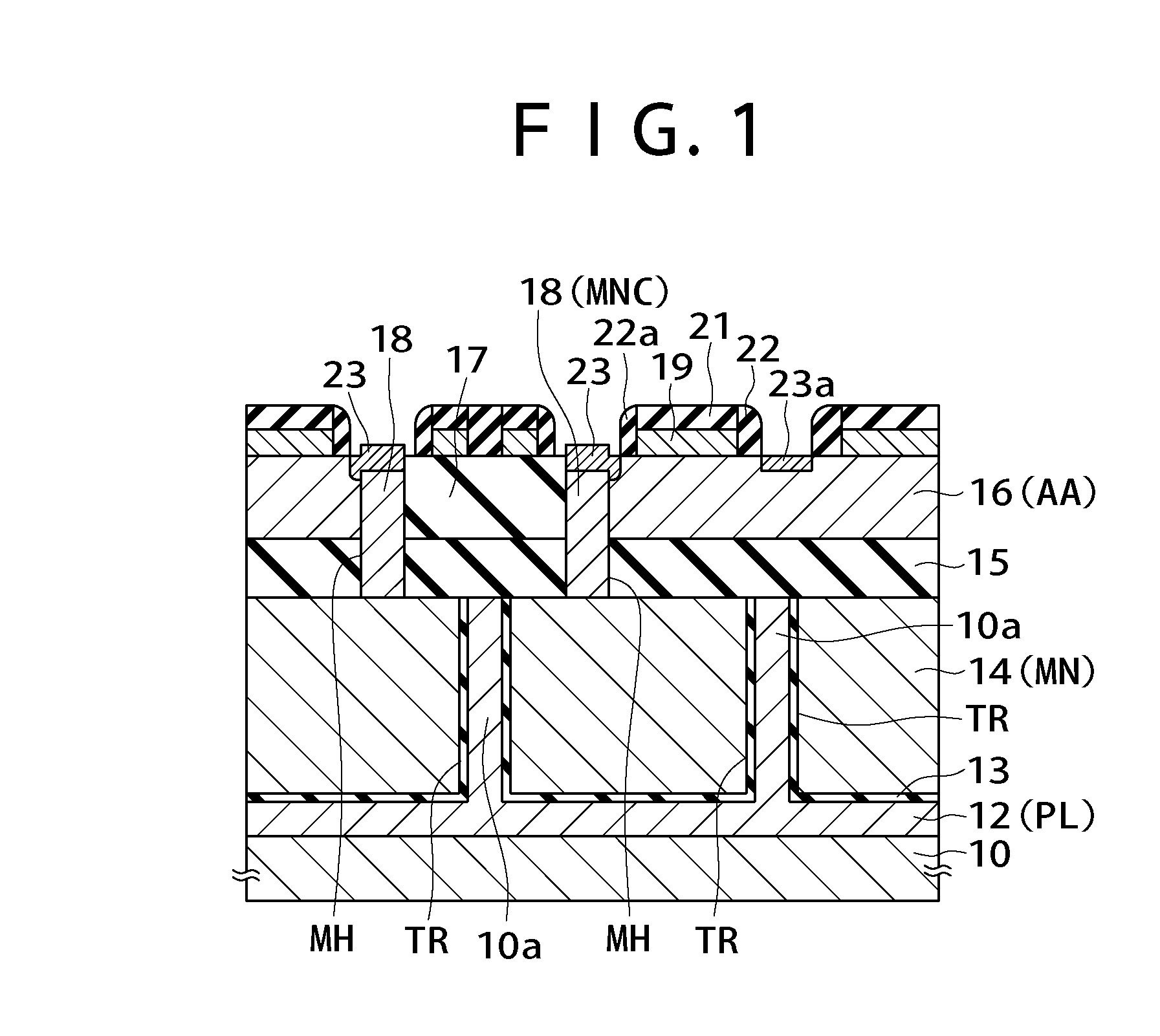
[0123]FIG. 8 is a sectional view of the memory cell of the DRAM pertaining to the present invention.

[0124] This DRAM is substantially identical with that in the first embodiment, except that the offset insulating film on the gate electrode 19 does not exist, the side wall insulating film 24 (with its surface retreated) exists on both sides of the gate electrode 19 which are close to the memory node contact and the bit contact, and the metal silicide layer 19a exists also on the surface of the gate electrode 19.

[0125] The DRAM according to this embodiment is characterized in that the source-drain (close to the memory node contact plug MNC) of the MOSFET formed in the third n-type semiconductor layer 16 is connected to the memory node contact plug MNC by the metallized region (or the metal silicide layer 23) in place of an impurity diffused from the memory node contact plug MNC. This structure obviates the necessity for heat treatment for impurity diffusion from the memory node cont...

third embodiment

[0139]FIG. 11 is a sectional view showing the important parts of the memory cell of the DRAM pertaining to this embodiment.

[0140] This DRAM is substantially identical with that in the first embodiment, except that the cylindrical insulating film 18b is formed on the surface of the side wall of the memory node contact hole MH and the memory node contact plug 18 is formed inside the cylindrical insulating film 18b.

[0141] The cylindrical insulating film 18b has a thickness L1 which is about 1 nm. The cylindrical insulating film 18b completely prevents impurities from diffusing from the fourth semiconductor layer 18 (memory node contact plug MNC) to the third n-type semiconductor layer 16. Thus no distance is necessary for alignment of lithography to make the contact hole and lithography to form the gate electrode. The result is a cell array with a reduced area.

[0142] On the channel forming region of the third n-type semiconductor region 16 are the gate electrode 19 and the offset in...


PUM


Abstract

Disclosed are a semiconductor memory device, a semiconductor device, and a method for production thereof. The semiconductor memory device and semiconductor device do not need for a distance for alignment of lithography to make the contact hole with lithography to form the gate electrode. Hence the resulting devices have a reduced area for the cell array. The semiconductor memory device is composed of a substrate having trenches formed side by side, a plate electrode which is formed to a prescribed depth from the surface of the inner wall of the trench, a capacitor insulating film which covers the surface of the inner wall of the trench, a memory node electrode MN which fills the trench, with the capacitor insulating film interposed between them, and a memory node contact plug which is buried in a contact hole which is so made as to reach the memory node electrode from the surface of the semiconductor layer. A metallized region is integrally formed to connect at least part of the surface of the semiconductor layer and at least part of the surface of the contact plug to each other.

Description

RELATED APPLICATION DATA [0001] This application is a divisional of U.S. patent application Ser. No. 11 / 024,901, filed Dec. 29, 2004, which is incorporated herein by reference to the extent permitted by law. This application claims the benefit of priority to Japanese Patent Application No. JP 2004-009319 filed in the Japanese Patent Office on Jan. 16, 2004, which is incorporated herein to the extent permitted by law.BACKGROUND OF THE INVENTION [0002] The present invention relates to a semiconductor memory device, a semiconductor device, and a method for production thereof. More particularly, the present invention relates to a semiconductor memory device, a semiconductor device, and a method for production thereof, the semiconductor having a memory node contact or other contacts for DRAM (dynamic random access memory). [0003] The recent advance in semiconductor devices (such as VLSI) is remarkable. In the last three years, they have decreased in size by 70 percent and increased in th...

Claims


Application Information

Patent Timeline
Patent Type & Authority Applications(United States)
IPC IPC(8): H01L21/8242H01L21/20H01L27/108H01L21/8234H01L21/8244H01L21/84H01L27/12H01L29/76H01L31/119
CPCH01L21/84H01L27/1203H01L27/10867H01L27/10832H10B12/373H10B12/0385H10B99/00
Inventor FUKUZAKI, YUZOTAKAHASHI, HIROSHI
Owner SONY CORP
Why Eureka
Try Eureka