Novel method to implement stress free polishing

a technology of stress-free polishing and polishing ring, which is applied in the direction of semiconductor/solid-state device manufacturing, basic electric elements, electric apparatus, etc., can solve the problems of increasing capacitance coupling between conductors, increasing power consumption, and even smaller dimensions of geometries, so as to achieve the maximum performance of the resulting semiconductor structure and reduce production costs

Inactive Publication Date: 2006-12-07
TAIWAN SEMICON MFG CO LTD
View PDF7 Cites 35 Cited by
  • Summary
  • Abstract
  • Description
  • Claims
  • Application Information

AI Technical Summary

Benefits of technology

[0012] In accordance with yet another aspect of the present invention, the steps of forming a metal layer/layers and stress free polishing the metal layer/layers are preferably performed in an integrated apparatus so that maximum performance of the resulting ...

Problems solved by technology

While in the past such reductions were limited only by the ability to define the structures photo-lithographically, device geometries having even smaller dimensions created new limiting factors.
This increased capacitance results in increased capacitive coupling between the conductors, increased power consumption, and an increase in the resistive-capacitive (RC) time constant.
However, porous dielectrics are mechanically weak by nature.
Weak dielectrics would fail in the chemical mechanical...

Method used


Image

  • Novel method to implement stress free polishing
  • Novel method to implement stress free polishing
  • Novel method to implement stress free polishing

Examples


Embodiment Construction

[0018] The making and using of the presently preferred embodiments are discussed in detail below. It should be appreciated, however, that the present invention provides many applicable inventive concepts that can be embodied in a wide variety of specific contexts. The specific embodiments discussed are merely illustrative of specific ways to make and use the invention, and do not limit the scope of the invention.

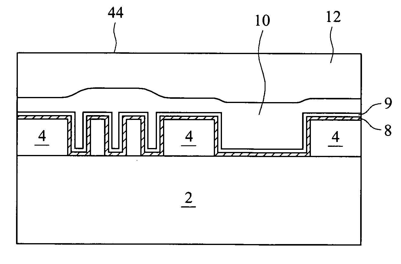
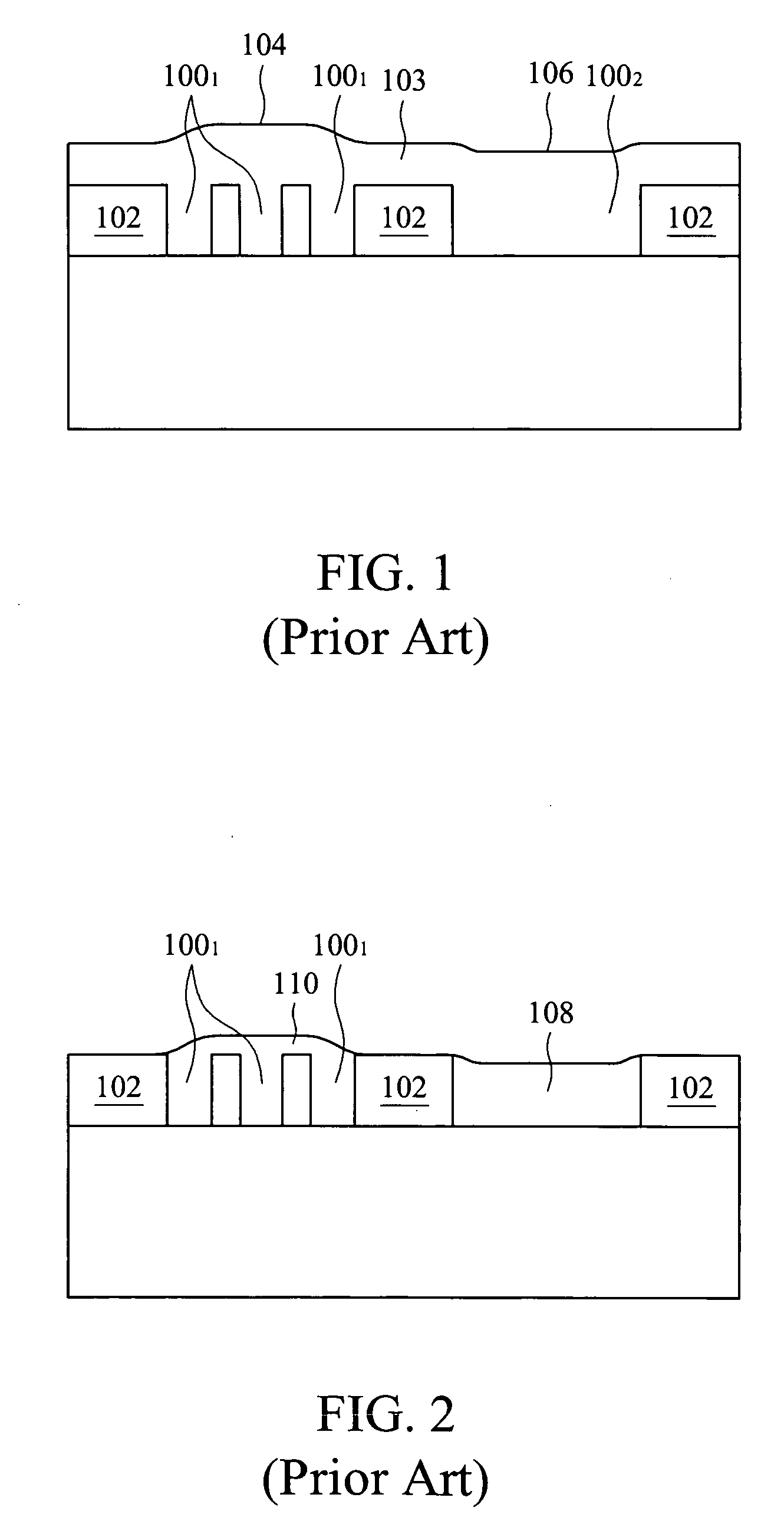
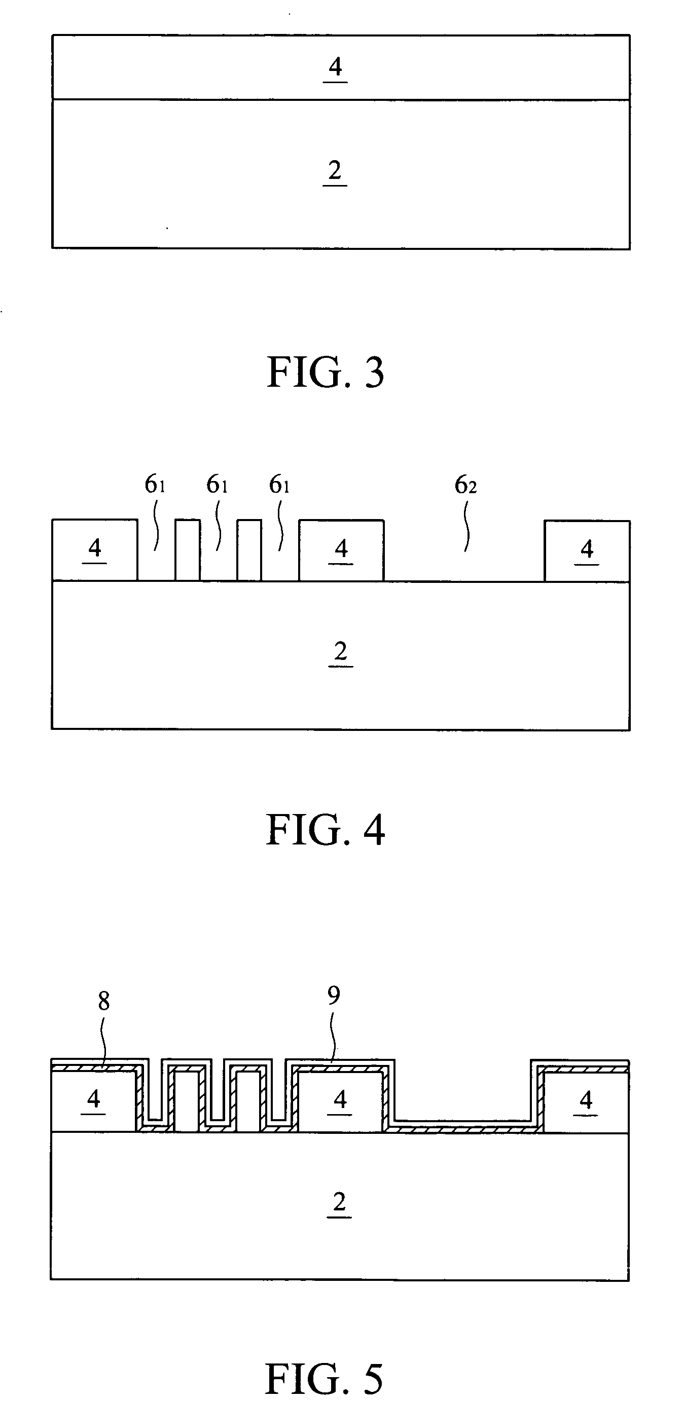
[0019] In semiconductor integrated circuit manufacturing processes, semiconductor devices are formed in / on a substrate. Metal features, such as metal lines, vias, and contacts, are used to interconnect devices. Metal features may be formed in different layers and separated by inter-layer dielectrics (ILD), also called inter-metal dielectrics (IMD). Damascene processes become common practices in the formation of metal features, particular for forming copper lines and vias. For discussion purposes, copper is referred to as the conductive material in the damascene processes th...


PUM


Abstract

A method of forming a metal feature in a low-k dielectric layer is provided. The method includes forming an opening in a low-k dielectric layer, forming a metal layer having a substantially planar surface over the low-k dielectric layer using spin-on method, and stress free polishing the metal layer. Preferably, the metal layer comprises copper or copper alloys. The metal layer preferably includes a first sub layer having a substantially non-planar surface and a second sub layer having a substantially planar surface on the first sub layer.

Description

TECHNICAL FIELD [0001] This invention relates generally to semiconductor processes, and specifically to damascene processes that include stress free polishing. BACKGROUND [0002] As the semiconductor industry introduces new generations of integrated circuits (IC's) having higher performance and greater functionality, the density of the elements that form the integrated circuits is increased, and the dimensions, sizes and spacing between the individual components or elements are reduced. While in the past such reductions were limited only by the ability to define the structures photo-lithographically, device geometries having even smaller dimensions created new limiting factors. For example, for any two adjacent conductive paths, as the distance between conductors decreases, the resulting capacitance (a function of the dielectric constant (k) of the insulating material divided by the distance between conductive paths) increases. This increased capacitance results in increased capaciti...

Claims


Application Information

Patent Timeline
IPC IPC(8): H01L21/4763
CPCH01L21/02068H01L21/32115H01L21/76877H01L21/76843H01L21/7684
Inventor WANG, JEANYANG, CHIA-MINGLO, HENRYTSENG, JOSHUA
Owner TAIWAN SEMICON MFG CO LTD
Why Eureka
Try Eureka