Semiconductor device with improved design freedom of external terminal

a technology of external terminals and semiconductors, applied in semiconductor devices, semiconductor/solid-state device details, electrical apparatus, etc., can solve the problems of difficult to form 300 external terminals on the surface area of a 7 mm7 mm wcsp, severe restriction of design freedom, and large volume of external terminals, etc., to achieve the effect of increasing the design freedom of disposal positions, and increasing the number of functions

Inactive Publication Date: 2006-12-14
LAPIS SEMICON CO LTD
View PDF19 Cites 4 Cited by
  • Summary
  • Abstract
  • Description
  • Claims
  • Application Information

AI Technical Summary

Benefits of technology

[0025] According to the constitution of the semiconductor device of this invention, external terminals can also be provided in a region including the upper side of the extension portion which is provided surrounding the semiconductor chip, and thus a semiconductor device with increased design freedom in the disposal pitch, disposal positions, and so on of the external terminals can be provided. Moreover, by applying a so-called WCSP manufacturing process, the semiconductor device of this invention can be constituted without the use of an interposer such as a substrate. As a result, improvements in operational speed, functional sophistication, number of functions, and compactness can be achieved in comparison with a device in which a wire bonding connection is employed. Further, an equal electrical characteristic can be achieved at a lower cost than a device in which a flip-chip connection is employed.
[0103] According to this manufacturing method for the semiconductor device of this invention, a semiconductor device can be provided by means of a simple process and with a greater functional sophistication, number of functions, and compactness. In particular, design freedom in the disposal pitch, disposal positions, and so on of the external terminals can be greatly increased.

Problems solved by technology

As shall be described below, however, design freedom is severely restricted by the disposal pitch and disposal positions of external terminals.
However, it is extremely difficult to form 300 external terminals on the surface area of a 7 mm×7 mm WCSP.
Since both of these connection methods utilize a substrate, and since additional sealing material is required in accordance with the height of the wire loop, the package becomes thick.
Moreover, the package becomes expensive due to the cost of the substrate.
The package becomes particularly expensive when a flip chip connection is used since an expensive buildup substrate is required.

Method used


Image

  • Semiconductor device with improved design freedom of external terminal
  • Semiconductor device with improved design freedom of external terminal
  • Semiconductor device with improved design freedom of external terminal

Examples


first embodiment

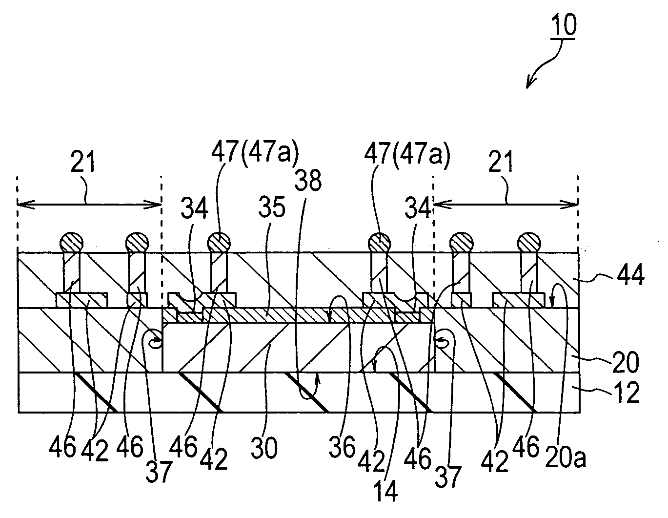
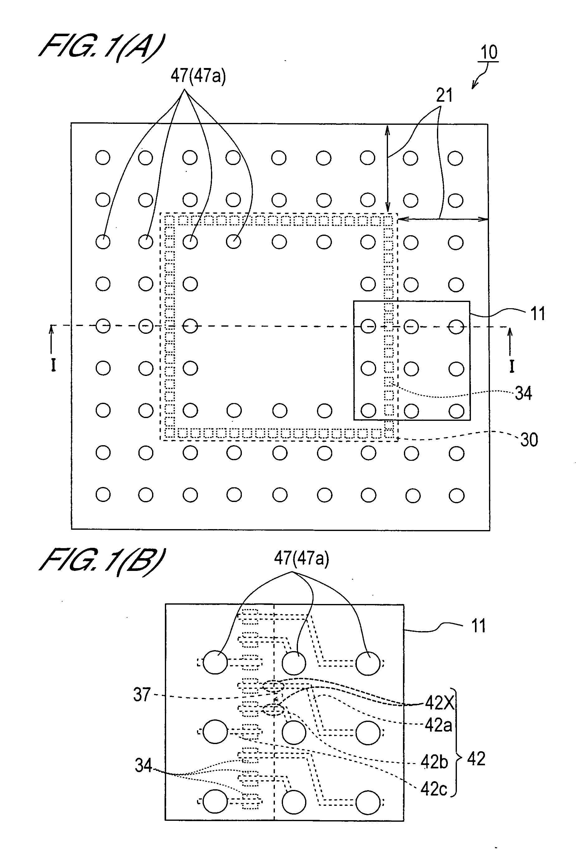
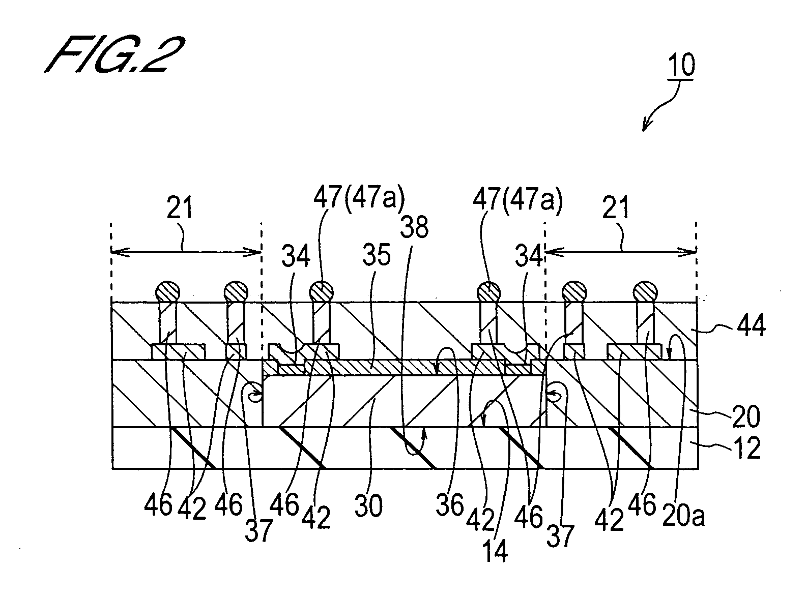
[0121] A semiconductor device according to a first embodiment of this invention will now be described with reference to FIGS. 1 and 2. FIG. 1(A) is a plan view seen from above showing in outline the constitution of the semiconductor device of the first embodiment, and FIG. 1(B) is a plan view showing an expanded outline of the main parts of a partial region of FIG. 1(A) in order to illustrate the connection relationship between a wiring pattern and electrode posts. FIG. 2 is a schematic sectional view showing a cross section severed along a broken line I-I in FIG. 1(A).

[0122] A semiconductor device 10 of the first embodiment of this invention comprises a semiconductor chip 30 on a base 12.

[0123] The base 12 may be appropriately selected as desired from a plate-form or sheet-form body made of an organic material such as a glass epoxy or a polyimide, for example, or a ceramic substrate, a metallic substrate, an Si substrate, or similar. A metallic substrate is preferably selected in...

second embodiment

[0185] A semiconductor device according to a second embodiment of this invention and a manufacturing method therefor will now be described with reference to FIGS. 10 through 12. Note that in the manufacturing process to be described below, applied materials, process implementation conditions, and so on are substantially identical to those of the first embodiment, and hence detailed description thereof has been omitted. Note also that in each drawing, the plan view is similar to that described in the first embodiment, and hence detailed description thereof has also been omitted.

[0186] A semiconductor device according to the second embodiment of this invention will now be described with reference to FIG. 10. FIG. 10 is a schematic sectional view of the semiconductor device of the second embodiment.

[0187] The semiconductor device 10 according to the second embodiment of this invention comprises a base 12. A semiconductor chip disposal region 14 is set on the base 12.

[0188] An insula...

third embodiment

[0235] A semiconductor device according to a third embodiment of this invention will now be described with reference to FIGS. 13(A) through 13(D). In addition to the constitution of the semiconductor devices 10 of the first and second embodiments described above, the semiconductor device 10 of the third embodiment has an insulating film 40 formed on a first surface 20a of an extension portion 20 and a surface protecting film 35 of a semiconductor chip 30. Inside walls 24 having an inclined form such that the extension portion 20 becomes gradually thinner toward the semiconductor chip 30 side are also provided.

[0236] Note that in the manufacturing process to be described below, applied materials, process implementation conditions, and so on are substantially identical to those described in the first embodiment, and hence detailed description thereof has been omitted. Note also that in each drawing, the plan view is similar to that described in the first embodiment, and hence illustr...


PUM


Abstract

A semiconductor device comprises: a base; a semiconductor chip provided on the base which includes a first main surface 20a on which a plurality of electrode pads is provided, a surface protecting film provided on the first main surface, a second main surface which opposes the first main surface, and a plurality of side surfaces between the surface of the surface protecting film and the second main surface; an insulating extension portion formed so as to surround the side surfaces of the semiconductor chip; a plurality of wiring patterns electrically connected to the electrode pads, respectively and extended from the electrode pads to the surface of the extension portion; a sealing portion formed on the wiring patterns such that a part of each of the wiring patterns is exposed; and a plurality of external terminals provided on the wiring patterns in a region including the upper side of the extension portion.

Description

BACKGROUND OF THE INVENTION [0001] 1. Field of the Invention [0002] This invention relates to a semiconductor device, and more particularly to a semiconductor device in which the degree of design freedom of an external terminal is increased in accordance with further increases in the number of external terminals. [0003] 2. Description of Related Art [0004] Demands have been made in recent years for further reductions in the size and thickness of packaged semiconductor devices. In response to such demands, a packaging form known as a Wafer Level Chip Size Package (to be referred to simply as WCSP hereinafter), in which the external size of the packaging is substantially equal to the external size of the semiconductor chip, has been proposed. [0005] A WCSP comprises a semiconductor chip. The semiconductor chip comprises a circuit element having a predetermined function and a plurality of electrode pads electrically connected to each other on the circuit element. An insulating film is ...

Claims


Application Information

Patent Timeline
Patent Type & Authority Applications(United States)
IPC IPC(8): H01L23/053H01L23/12H01L23/538
CPCH01L23/5389H01L23/3135H01L24/97H01L2224/04105H01L2224/20H01L2224/211H01L2224/97H01L2924/01004H01L2924/01013H01L2924/01029H01L2924/01078H01L2924/01079H01L2924/01082H01L2924/30107H01L24/19H01L2224/73267H01L2924/01005H01L2924/01006H01L2924/01033H01L2224/32225H01L2224/32245H01L2224/82H01L2924/15787H01L2924/181H01L2924/351
Inventor WATANABE, KIYONORI
Owner LAPIS SEMICON CO LTD
Why Eureka
Try Eureka