Method of removing the growth substrate of a semiconductor light emitting device

a light-emitting device and growth substrate technology, applied in the field of light-emitting devices, can solve the problems of poor extraction efficiency and degrading the performance of the devi

Active Publication Date: 2006-12-14
LUMILEDS
View PDF16 Cites 148 Cited by
  • Summary
  • Abstract
  • Description
  • Claims
  • Application Information

AI Technical Summary

Benefits of technology

[0009] In accordance with embodiments of the invention, a semiconductor structure formed on a growth substrate and including a light emitting layer disposed between an n-type region and a p-type region is attached to a carrier by a connection that supports the semiconductor structure sufficiently to permit removal of the growth substrate. In some embodiments, the semiconductor structure is a III-nitride flip chip device. The semiconductor structure may be attached to the carrier by, for example, a metal bond that supports almost the entire lateral extent of the semiconductor structure, or by interconnects such as solder or gold stud bumps. An underfill material which supports the semiconductor structure is introduced in the space between the interconnects. In some embodiments, the underfill is a soft material such as a liquid that is introduced between the carrier and the semiconductor structure, then cured to form a rigid structure. The growth substrate may then be removed without causing damage to the semiconductor structure.
[0010] In some embodiments, after the growth substrate is removed, a wavelength converting material such as a phosphor is disposed on the surface of the semiconductor structure exposed by substrate removal. The underfill may be disposed along the sides of the semiconductor structure and the growth substrate, such that an enclosure is formed by the underfill remaining when the growth substrate is removed. The enclosure may contain the wavelength converting material. The underfill introduced between the semiconductor structure and the carrier, the underfill disposed along the sides of the semiconductor structure, and the wavelength converting material disposed on the top surface of the semiconductor structure form a seal which protects the semiconductor structure.

Problems solved by technology

In a flip chip device, the use of a sapphire substrate may lead to poor extraction efficiency due to the large difference in index of refraction at the interface between the semiconductor layers and the substrate.
Laser dissociation in particular generates shock waves in the semiconductor layers which can damage the semiconductor or metallization layers, potentially degrading the performance of the device.

Method used


Image

  • Method of removing the growth substrate of a semiconductor light emitting device
  • Method of removing the growth substrate of a semiconductor light emitting device
  • Method of removing the growth substrate of a semiconductor light emitting device

Examples


Embodiment Construction

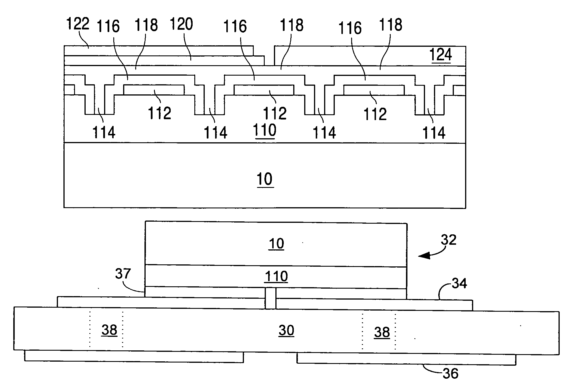
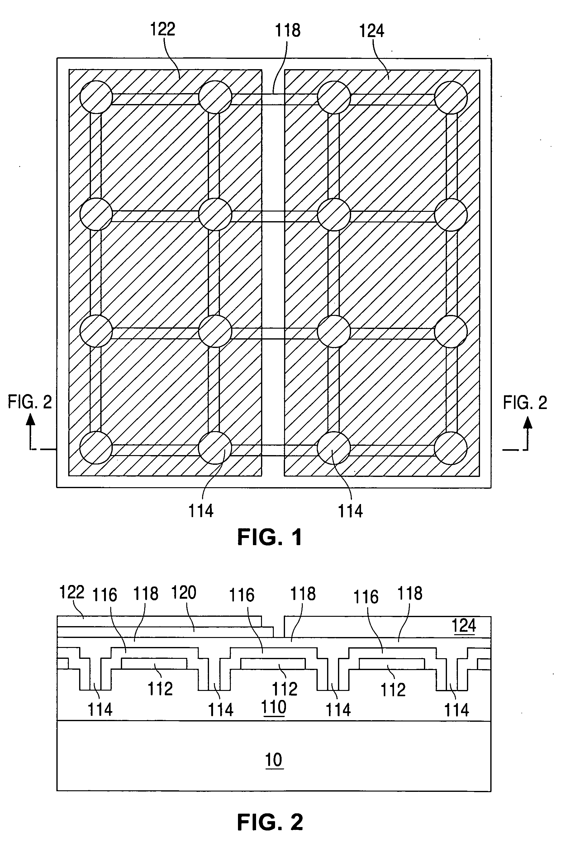
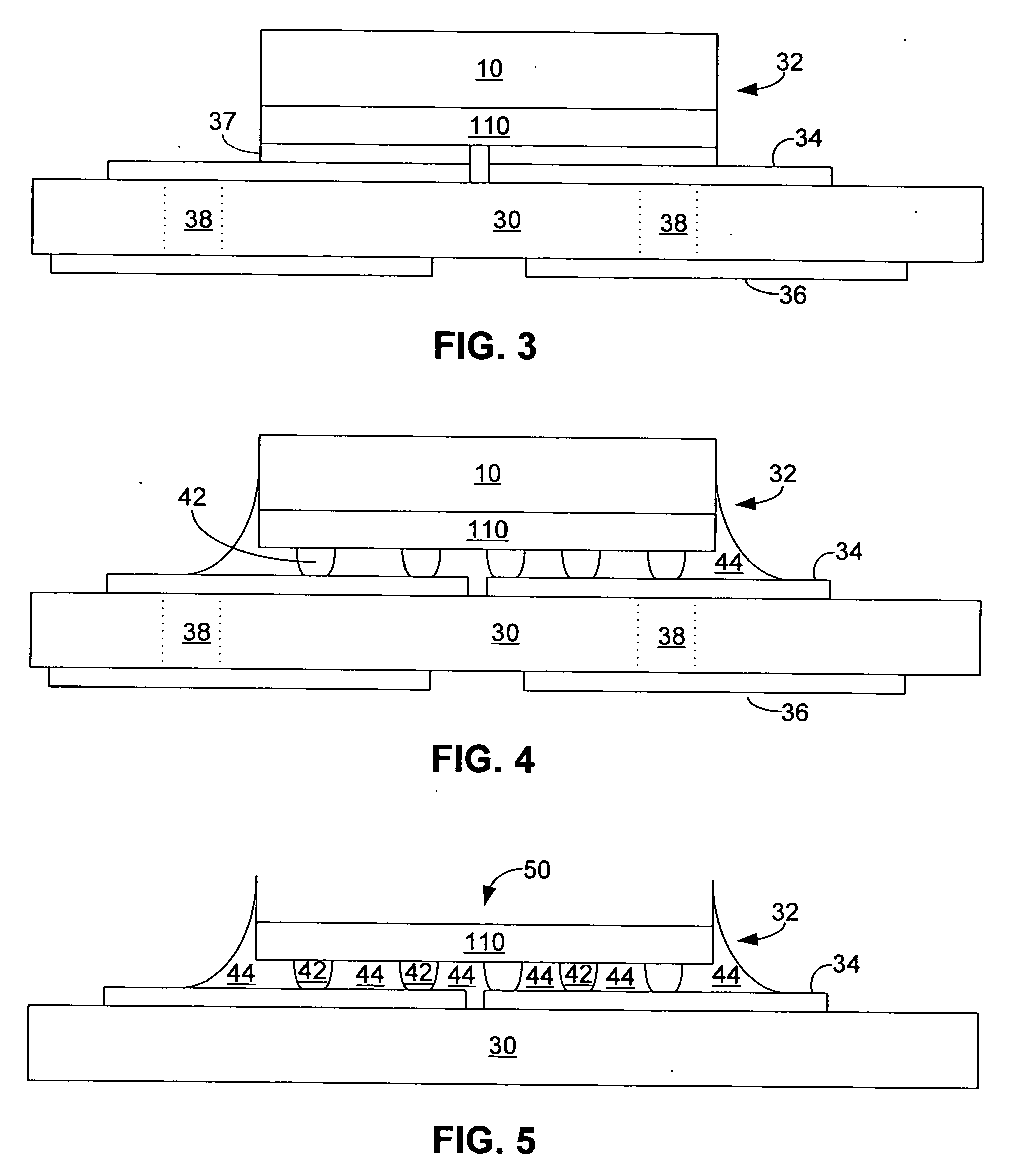
[0021] In accordance with embodiments of the invention, a semiconductor light emitting device is attached to a carrier by a connection that permits removal of the growth substrate. Though the examples below describe flip chip semiconductor light emitting device, embodiments of the invention may be applied to vertical semiconductor light emitting devices, where the first electrical contact is disposed on a bottom side of the semiconductor structure and the second contact is disposed on the top side of the semiconductor structure.

[0022] A standard epitaxial structure is first grown on a growth substrate. In III-nitride devices, an n-type region is typically grown first over the growth substrate. The n-type region may include multiple layers of different composition and dopant concentration, including, for example, preparation layers such as buffer layers or nucleation layers which may be n-type or not intentionally doped, release layers designed to facilitate release of the growth su...


PUM


Abstract

A semiconductor structure formed on a growth substrate and including a light emitting layer disposed between an n-type region and a p-type region is attached to a carrier by a connection that supports the semiconductor structure sufficiently to permit removal of the growth substrate. In some embodiments, the semiconductor structure is a flip chip device. The semiconductor structure may be attached to the carrier by, for example, a metal bond that supports almost the entire lateral extent of the semiconductor structure, or by interconnects such as solder or gold stud bumps. An underfill material which supports the semiconductor structure is introduced in any spaces between the interconnects. The underfill material may be a liquid that is cured to form a rigid structure. The growth substrate may then be removed without causing damage to the semiconductor structure.

Description

BACKGROUND [0001] 1. Field of Invention [0002] This invention relates to light emitting devices such as light emitting diodes (LEDs) and, in particular, to techniques for mounting LEDs for packaging and for removing the growth substrate of the LEDs. [0003] 2. Description of Related Art [0004] Semiconductor light-emitting devices including light emitting diodes are among the most efficient light sources currently available. Materials systems currently of interest in the manufacture of high-brightness light emitting devices capable of operation across the visible spectrum include Group III-V semiconductors, particularly binary, ternary, and quaternary alloys of gallium, aluminum, indium, and nitrogen, also referred to as III-nitride materials. Typically, III-nitride light emitting devices are fabricated by epitaxially growing a stack of semiconductor layers of different compositions and dopant concentrations on a sapphire, silicon carbide, III-nitride, or other suitable substrate by m...

Claims


Application Information

Patent Timeline
Patent Type & Authority Applications(United States)
IPC IPC(8): H01L21/00H01L33/00
CPCH01L33/0079H01L33/20H01L33/382H01L24/97H01L2924/12041H01L2224/32225H01L2224/73204H01L2224/97H01L2224/16225H01L2224/81H01L2924/00H01L33/0093H01L2924/00011H01L2924/00014H01L2924/12042H01L2224/0401
Inventor EPLER, JOHN E.SHOHEKIN, OLEG B.WALL, FRANKLIN J. JR.WIERER, JONATHAN J. JR.ZHOU, LING
Owner LUMILEDS
Why Eureka
Try Eureka