Wafer dividing method

Active Publication Date: 2006-12-14
DISCO CORP
View PDF3 Cites 10 Cited by
  • Summary
  • Abstract
  • Description
  • Claims
  • Application Information

AI Technical Summary

Benefits of technology

[0008] It is an object of the present invention to provide a wafer dividing method capable of dividing a wafer into individual devices without being influenced by test metal patterns formed on the streets and preventing the constitution of the obtained devices from being detected.

Problems solved by technology

When TEGs are formed on the streets of the wafer, however, there is a problem that the TEGs interfere with the laser beam, thereby making it impossible to form a groove or deteriorated layer uniformly.
However, when the wafer having the grooves or deteriorated layers is divided by exerting external force thereto, there is a problem that a TEG is broken in a shape of sawteeth to generate dusts and consequently, causes contamination and reduces the quality of devices.
Further, as the TEGs remain on the obtained chips, it allows detecting the constitution of each device by using the remaining TEG, resulting in the leakage of a company secret.

Method used


Image

  • Wafer dividing method
  • Wafer dividing method
  • Wafer dividing method

Examples


first embodiment

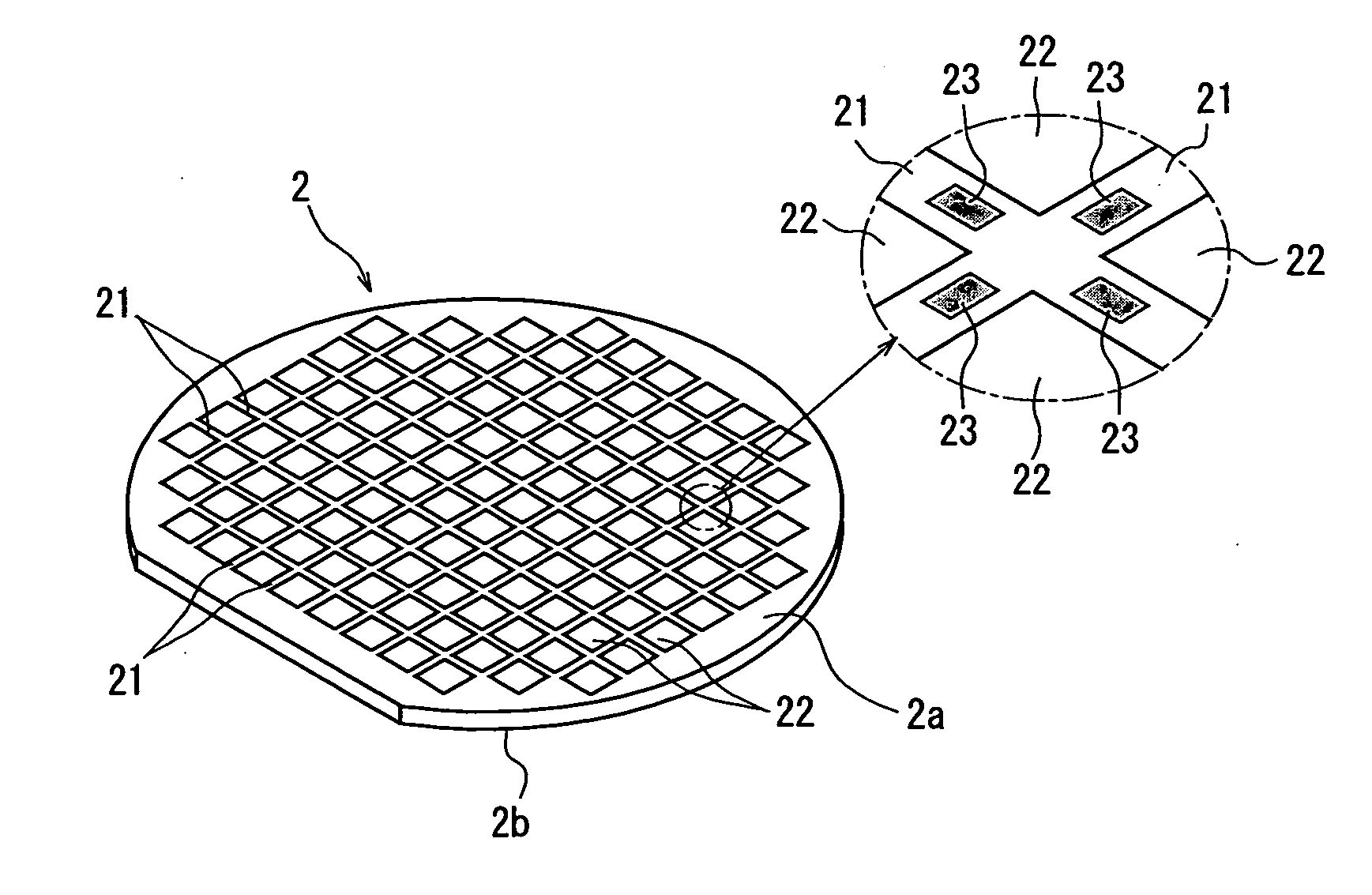
[0038] A description will be first given of the method of dividing the semiconductor wafer 2 along the plurality of streets 21.

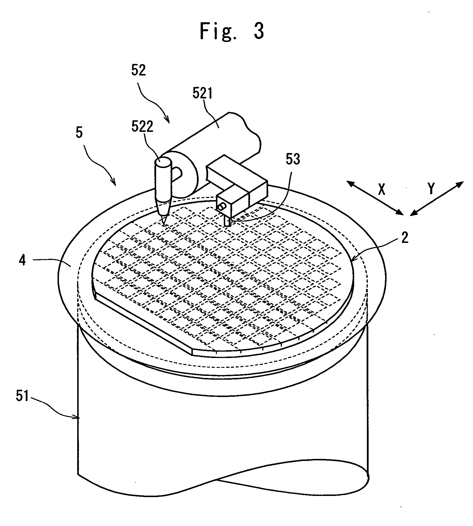
[0039] First comes a laser beam application step for carrying out laser processing by applying a laser beam along a street 21 on both sides of the test metal patterns 23 in the street 21 formed on the semiconductor wafer to form a dividing start point along the street 21 on both sides of the test metal patterns 23. This laser beam application step is carried out by using a laser beam processing machine shown in FIG. 3. The laser beam processing machine 5 shown in FIG. 3 comprises a chuck table 51 for holding a workpiece and laser beam application means 52 for applying a laser beam to the workpiece held on the chuck table 51. The chuck table 51 is so constituted as to suction-hold the workpiece and is designed to be moved in a processing-feed direction indicated by an arrow X in FIG. 3 by a processing-feed mechanism (not shown) and an indexing-feed direction ...

second embodiment

[0059] A description will be subsequently given of the wafer dividing method with reference to FIGS. 10(a), 10(b), 11(a), 11(b), 12(a) and 12(b).

[0060] In the embodiment shown in FIGS. 10(a) and 10(b) and FIGS. 11(a) and 11(b), a groove is formed as a dividing start point along a street 21 on both sides of the test metal patterns 23 in the street 21 by using a pulse laser beam of a wavelength having absorptivity for the semiconductor wafer 2. In this embodiment, the back surface 2b side of the semiconductor wafer 2 is put on the surface of the protective tape 4 mounted on the annular frame 3. Therefore, the front surface 2a of the semiconductor wafer 2 faces up.

[0061] After the street 21 formed on the semiconductor wafer 2 held on the chuck table 51 is detected and the alignment of the laser beam application position is carried out as described above, the chuck table 51 is moved to a laser beam application area where the condenser 522 of the laser beam application means 52 for appl...

third embodiment

[0071] A description will be subsequently given of the wafer dividing method of the present invention with reference to FIGS. 13(a) and 13(b) and FIG. 14.

[0072] First comes a first laser beam application step for carrying out laser processing by applying a laser beam along a street 21 on one side of the test metal patterns 23 in the street 21 formed on the semiconductor wafer 2 to form a dividing start point along the street 21 on one side of the test metal patterns 23 of the semiconductor wafer 2. This first laser beam application step may be identical to the above-described laser beam application step shown in FIGS. 4(a) and 4(b) and FIGS. 5(a) and 5(b).

[0073] After the above first laser beam application step is carried out to form a deteriorated layer 24 as a dividing start point along the street 21 on one side of the test metal patterns 23 in the street 21 formed on the semiconductor wafer 2, the chuck table 51, that is, the semiconductor wafer 2 is moved in the indexing-feed d...


PUM


Abstract

A method of dividing a wafer having a plurality of devices, which are formed in a plurality of areas sectioned by streets formed in a lattice pattern on the front surface, and having test metal patterns which are formed on the streets, comprising the steps of: a laser beam application step for carrying out laser processing to form a dividing start point along a street on both sides of the test metal patterns by applying a laser beam along the street on both sides of the test metal patterns in the street formed on the wafer; and a dividing step for dividing the wafer which has been laser processed to form dividing start points along the dividing start points by exerting external force to the wafer, resulting in leaving the streets having the test metal patterns formed thereon behind.

Description

FIELD OF THE INVENTION [0001] The present invention relates to a method of dividing a wafer having a plurality of devices, which are formed in a plurality of areas sectioned by streets formed in a lattice pattern on the front surface, and having test metal patterns which are formed on the streets. DESCRIPTION OF THE PRIOR ART [0002] As known to people of ordinary skill in the art, in the production process of a semiconductor device, individual semiconductor chips are manufactured by cutting a semiconductor wafer comprising devices such as IC's or LSI's which are formed in a plurality of areas sectioned by dividing lines called “streets” arranged in a lattice pattern on the front surface of a substantially disk-like semiconductor substrate along the streets to divide it into areas on which each of the device is formed. [0003] Most of the above semiconductor wafers have a plurality of test metal patterns called “test element group (TEG)” for testing the function of each device, on the...

Claims


Application Information

Patent Timeline
IPC IPC(8): H01L21/00B23K26/364
CPCB23K26/4075B28D5/0011H01L2221/68327H01L21/78H01L21/6836B23K26/40B23K2103/50
Inventor NAKAMURA, MASARUNAGAI, YUSUKE
Owner DISCO CORP
Why Eureka
Try Eureka