Short channel semiconductor device fabrication

a semiconductor device and short channel technology, applied in the field of short channel semiconductor device fabrication, can solve the problems of increasing off-state current, limiting the extent to which transistor dimensions can be reliably scaled, and performance limitations are also a barrier to scaling conventional planar transistor dimensions, so as to mitigate the establishment of a conduction path and short channel

Active Publication Date: 2006-12-14
TEXAS INSTR INC
View PDF9 Cites 12 Cited by
  • Summary
  • Abstract
  • Description
  • Claims
  • Application Information

AI Technical Summary

Benefits of technology

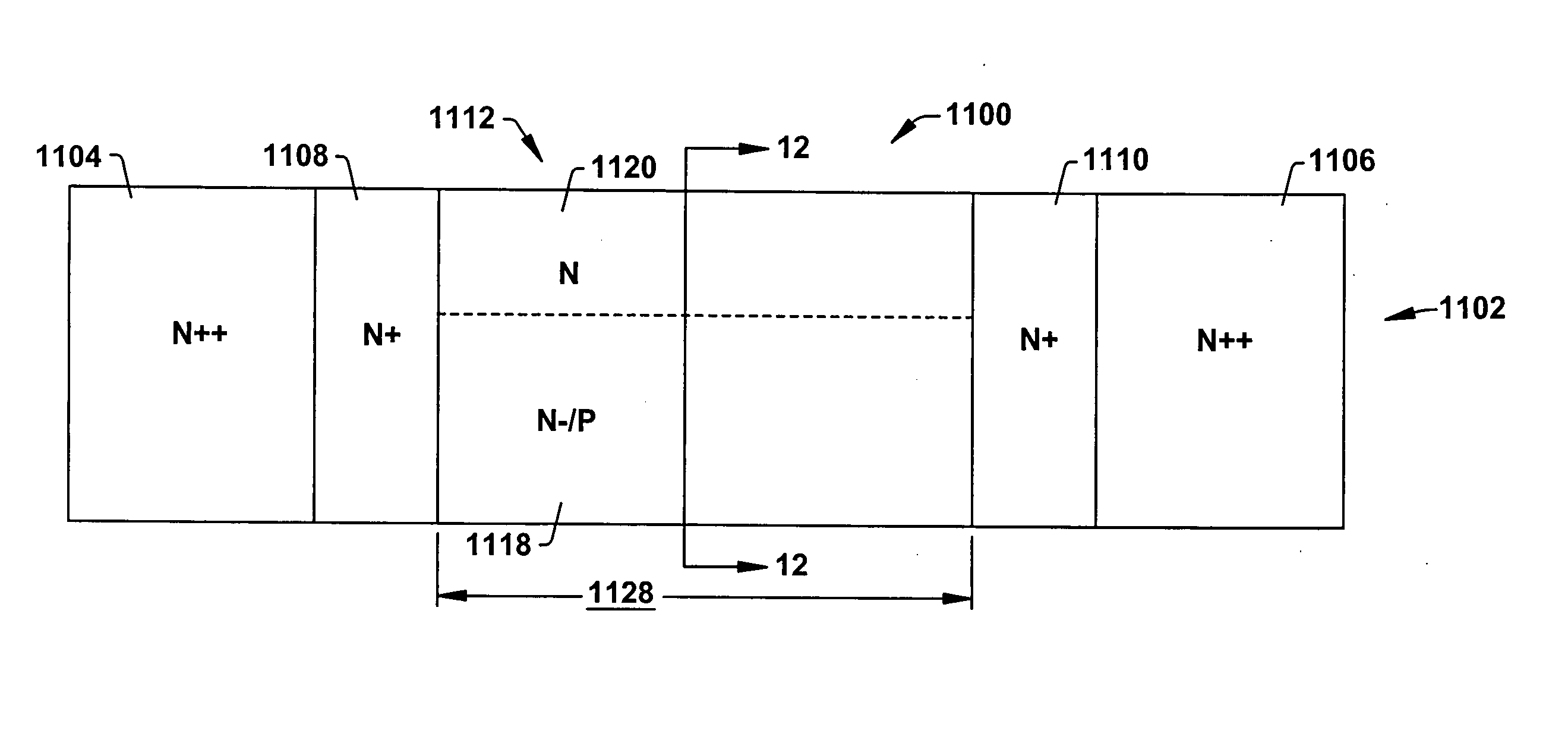
[0016] One or more aspects of the present invention pertain to forming accumulation mode multi gate transistor devices so that short channel effects are mitigated. In particular, one more types of dopant materials are implanted in a channel region, one or more extension regions and / or a source or drain region of the transistor to mitigate the establishment of a conduction path and the accumulation of electrons in the channel region that can result in an unwanted leakage current.

Problems solved by technology

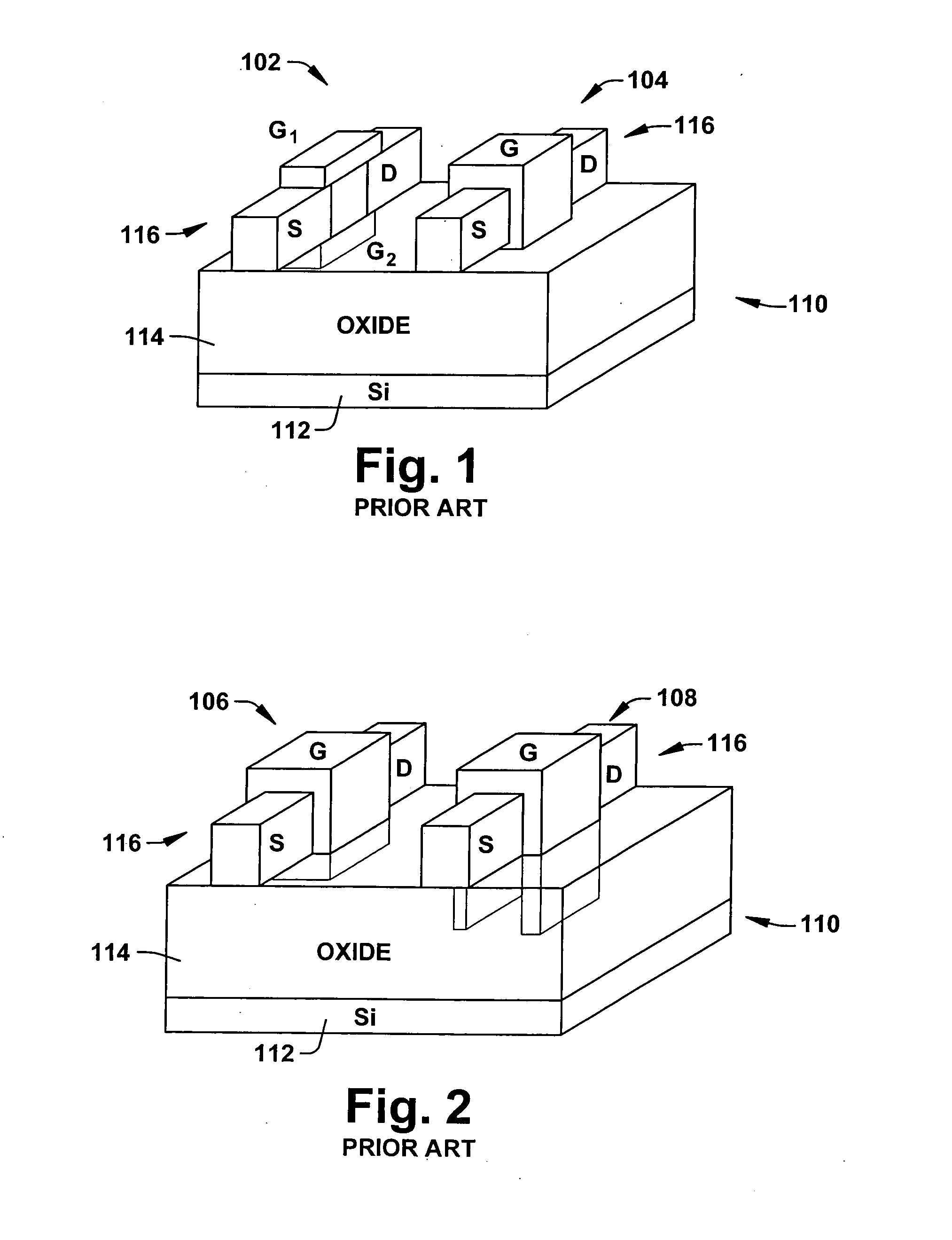
However, lithography generally limits the extent to which transistor dimensions can be reliably scaled, wherein the minimum gate length is typically limited to the smallest dimension that can be repeatably patterned and etched using current photolithographic and etching techniques.
In addition to fabrication process limitations, performance limitations are also a barrier to scaling conventional planar transistor dimensions, particularly the gate length.
In shorter channel devices, however, the channel region is also affected by the source and drain voltages, leading to increased off state current due to Vt roll off, degraded subthreshold slope, and degraded output current.
Accumulation mode transistor devices generally offer high current drive and reduced short channel effects, where the threshold voltage in such devices is limited by the amount of doping atoms that can be placed in the small channel region volume and by the choice of available gate materials.
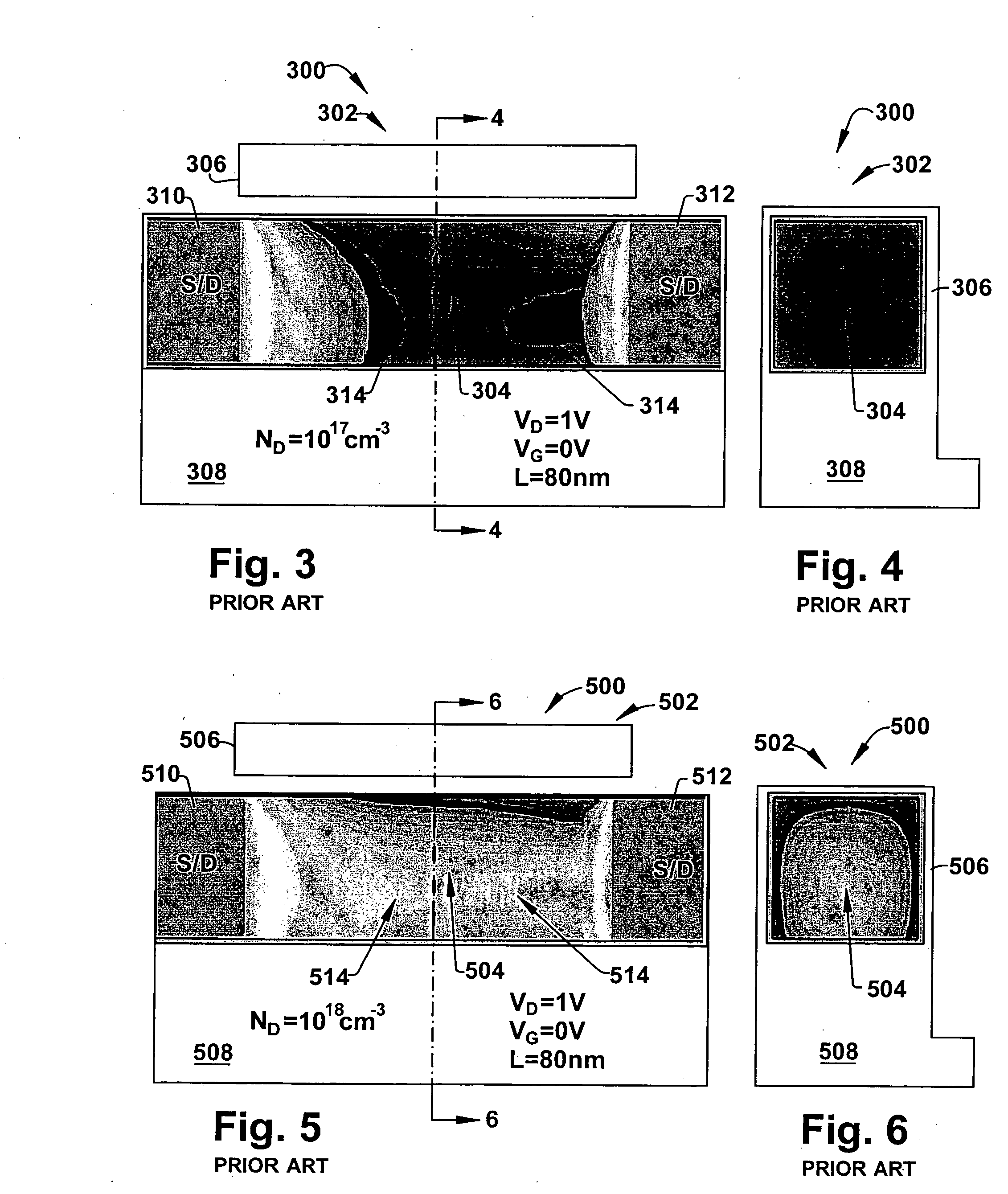
An increased dopant concentration, however, can result in a sufficient number of electrons (or electron concentration) being present in the channel region so that a leakage current develops in the channel region.
Nevertheless, this electron accumulation still may be insufficient for a leakage current to develop in the channel region 704 when the device 700 is off (VG=0V and VD=1V).

Method used


Image

  • Short channel semiconductor device fabrication
  • Short channel semiconductor device fabrication
  • Short channel semiconductor device fabrication

Examples


Embodiment Construction

[0052] One or more aspects of the present invention are described with reference to the drawings, wherein similar or like reference numerals or characters are generally utilized to refer to similar or like elements, structures, features, components, etc. throughout, and wherein what is depicted herein is not necessarily drawn to scale. It will be appreciated that where like acts, events, elements, features, layers, structures, etc. are reproduced, subsequent (redundant) discussions of the same may be omitted for the sake of brevity. In the following description, for purposes of explanation, numerous specific details are set forth in order to provide a thorough understanding of one or more aspects of the present invention. It may be evident, however, to one of ordinary skill in the art that one or more aspects of the present invention may be practiced with a lesser degree of these specific details. In other instances, known structures are shown in diagrammatic form in order to facili...


PUM


Abstract

The formation of one or more accumulation mode multi gate transistor devices is disclosed. The devices are formed so that short channel effects are mitigated. In particular, one more types of dopant materials are implanted in a channel region, an extension region and / or source / drain regions to mitigate the establishment of a conduction path and the accumulation of electrons in the channel region that can result in an unwanted leakage current.

Description

FIELD OF INVENTION [0001] The present invention relates generally to semiconductor devices, and more particularly to fabricating a semiconductor device having a short channel region. BACKGROUND OF THE INVENTION [0002] Metal oxide semiconductor field effect transistors (MOSFETs) are widely used in the electronics industry for switching, amplification, filtering, and other tasks related to both analog and digital electrical signals. Conventional planar MOS transistors include a gate structure or stack formed on a semiconductor substrate. The gate stack generally includes a thin gate dielectric overlying the substrate and a gate electrode situated over the gate dielectric. Source and drain regions are formed in the substrate on either side of the gate structure, thereby defining a channel region at the upper surface of the substrate under the gate structure. [0003] In operation, the gate electrode is energized to create an electric field in the channel region of the substrate, thus inv...

Claims


Application Information

Patent Timeline
Patent Type & Authority Applications(United States)
IPC IPC(8): H01L21/336
CPCH01L29/66651H01L29/66795H01L2029/7857H01L29/78621H01L29/785
Inventor COLINGE, JEAN-PIERREXIONG, WEIZE
Owner TEXAS INSTR INC
Why Eureka
Try Eureka