

Light emitting diode device using electrically conductive interconnection section
a technology of light-emitting diodes and electrically conductive sections, which is applied in the direction of semiconductor devices, basic electric elements, electrical apparatus, etc., can solve the problems of complex manufacturing process, difficulty in uniform dispersing of fluorescent substances, and difficulty in discharging. achieve the effect of enhancing the light extraction efficiency of light-emitting diodes
- Summary
- Abstract
- Description
- Claims
- Application Information
AI Technical Summary
Benefits of technology
Problems solved by technology
Method used
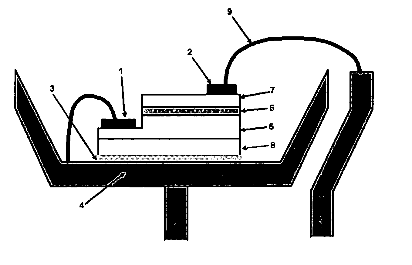
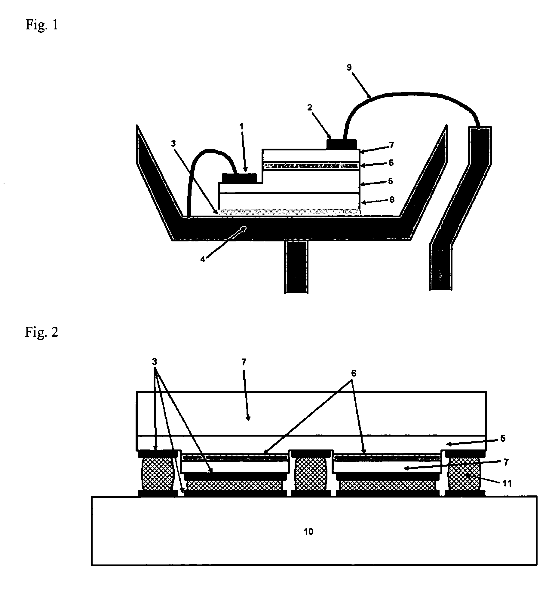
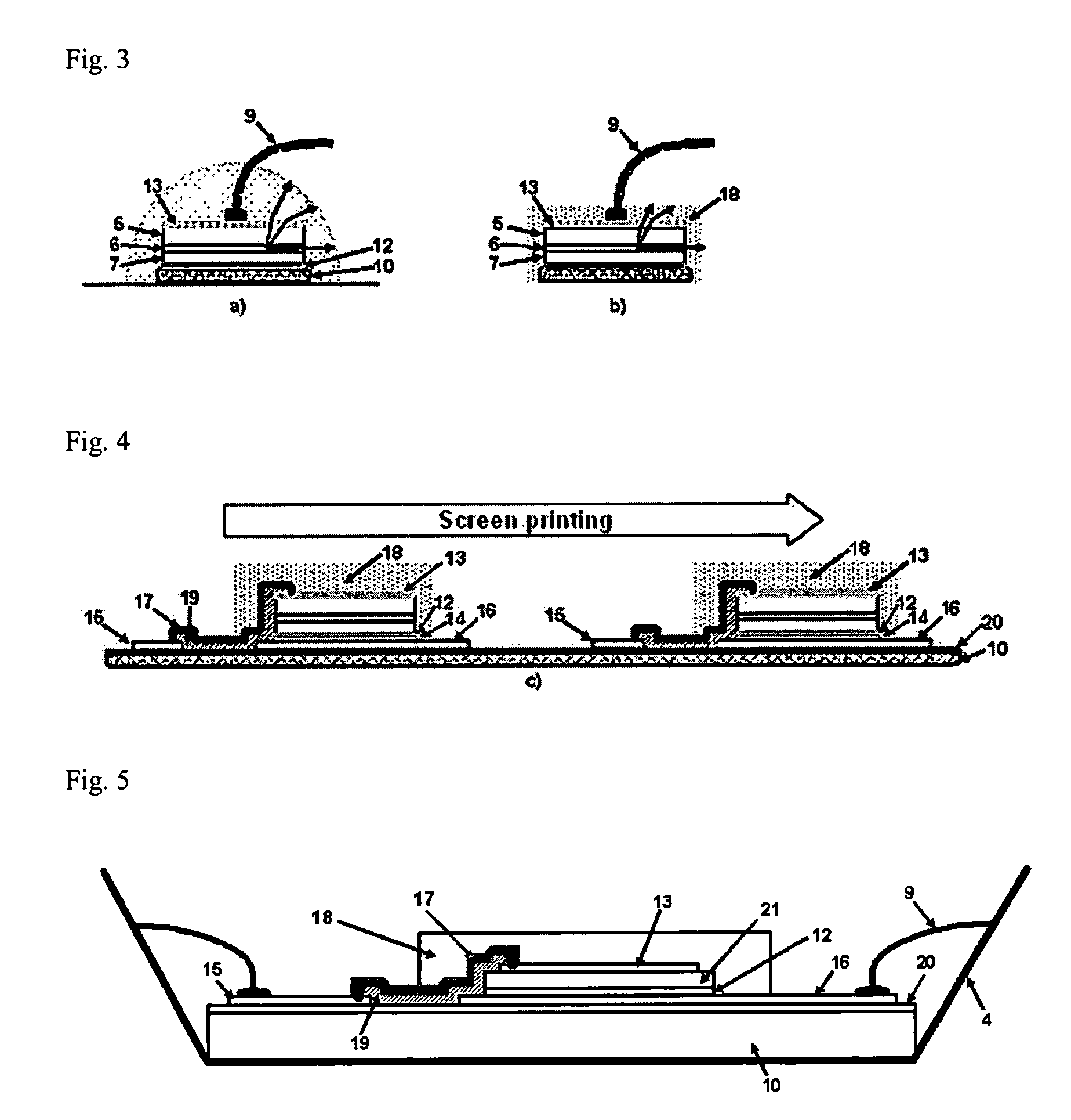
Image

Examples
example 1
Area Analysis of Wire Bonding Pad (Electrically Conductive Pad) for Wire 9 According to Change of Chip Area
[0109]FIG. 9 is a graph showing a ratio of an area occupied by the bonding pad for the wire 9 according to the change of the overall chip area. That is, FIG. 9 graphically shows by calculation how much the bonding pad existing over the light emitting diode covers light vertically emitted from the light emitting diode. In FIG. 9, since there is little difference between an area of covering the vertically emitted light by the wire 9 in a case where the wire bonding is performed directly in an upper portion of the light emitting diode and an area of covering the vertically emitted light by the interconnection section 17 in a case of using the interconnection section 17 structure, the difference between the two cases was neglected.
[0110] The number of the wire bonding pads varied between 1 and 10, and two conditions were considered for the area analysis. One of them is a conditio...
PUM
 Abstract
Description
Claims
Application Information