Capacitance modeling

Inactive Publication Date: 2006-12-21
GLOBALFOUNDRIES INC
View PDF6 Cites 7 Cited by
  • Summary
  • Abstract
  • Description
  • Claims
  • Application Information

AI Technical Summary

Benefits of technology

[0022] The method may also include fitting the capacitance expression to exact EM solver results for a subject structure to improve accuracy. The step of fitting may be performed by adding factors to the capacitance expressions for the structural components.

Problems solved by technology

The drawbacks of this prior art solution are as follows.
1) The interpolation is quite approximate, and its validity is severely limited to the range of geometries used in the numerical database.
2) It is very time consuming to build and run the numerical database repeatedly when using the models for a different silicon chip technology with different wire cross sectional dimensions and often with multiple metal stack options.
The main drawback of these solutions is that they are not physics based, and rather use several known functions (such as logarithmic functions, power functions, etc.) which limits their range of applicability.
However, this solution lacks flexibility since it is restricted to some specific cases and cannot be simply extended to include other structures.
608-611 for single signal line without side shields) which results in much more complicated expressions compared with a semi-analytical approach.

Method used


Image

  • Capacitance modeling
  • Capacitance modeling
  • Capacitance modeling

Examples


Embodiment Construction

[0027] Embodiments of the present invention will now be described, by way of examples only, with reference to the accompanying drawings in which:

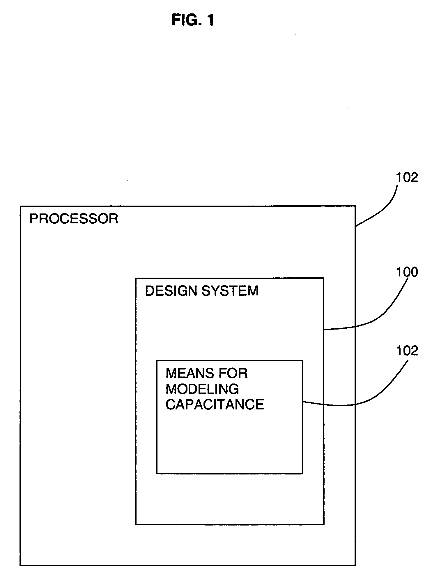
[0028]FIG. 1 is a schematic representation of an integrated circuit design system for implementing a design process including modeling capacitance in accordance with the present invention;

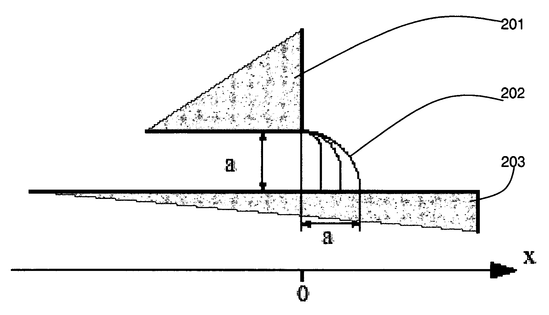
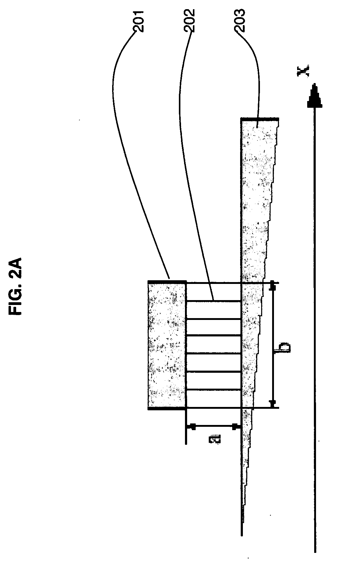
[0029]FIGS. 2A to 2E are five basic field line patterns used in accordance with the present invention;

[0030]FIGS. 3A to 3D are cross-sections of transmission line topologies used in accordance with the present invention;

[0031]FIGS. 4A and 4B show cross-sections of the topology of FIG. 3D divided into two single ground topologies in accordance with an aspect of the invention;

[0032]FIG. 5 is a cross-section of a transmission line showing the dimension references used in the description and equations;

[0033]FIG. 6 is a flow diagram of a method of modeling capacitance in accordance with an aspect of the present invention; and

[0034]FIGS. 7A and 7B are flo...


PUM


Abstract

A method of modeling capacitance for all practical 2D on-chip wire structures including coplanar and microstrip structures. The method includes using a field lines approach (600) to obtain capacitance expressions for structure components, combining the expressions (704) for components of the subject structure and obtaining a capacitance expression (705) for the subject structure. The static capacitance matrix for the structure is calculated from the capacitance expression. The structure components can include components with parallel plate field lines, quarter circle field lines, singularity field lines, singularity field lines with restriction, double set of quarter circle field lines which are used as building blocks for the subject structure. The final capacitance expressions can be used for the modeling of critical on-chip wires and devices as well as inside a capacitance extraction tool.

Description

TECHNICAL FIELD [0001] The present invention relates to the field of modeling capacitance. In particular, the invention relates to modeling and extraction of capacitance of wires in integrated circuits; specifically, modeling capacitance of on-chip transmission lines. BACKGROUND OF THE INVENTION [0002] Models of on-chip transmission lines have been developed as a part of the “T-lines set” which is the core of an interconnect-aware design and modeling methodology, enabling high predictability of the critical interconnect behaviour. Further information is provided in references: Goren, D. et al., “An Interconnect-Aware Methodology for Analog and Mixed Signal Design, Based on High Bandwidth (Over 40 GHz) On-chip Transmission Line Approach” IEEE DATE'02 Conference, Paris March 2002, pp. 804-811 and Goren, D. et al., “On-chip Interconnect-Aware Design and Modeling Methodology, Based on High Bandwidth Transmission Line Devices”, IEEE DAC'03 Conference, CA, June 2003, pp. 724-727. [0003] D...

Claims


Application Information

Patent Timeline
IPC IPC(8): H01L21/66
CPCG06F17/5036G06F30/367
Inventor GOREN, DAVIDSHLAFMAN, SHLOMO
Owner GLOBALFOUNDRIES INC
Why Eureka
Try Eureka