This helps you quickly interpret patents by identifying the three key elements:
Problems solved by technology
Method used
Benefits of technology
Benefits of technology
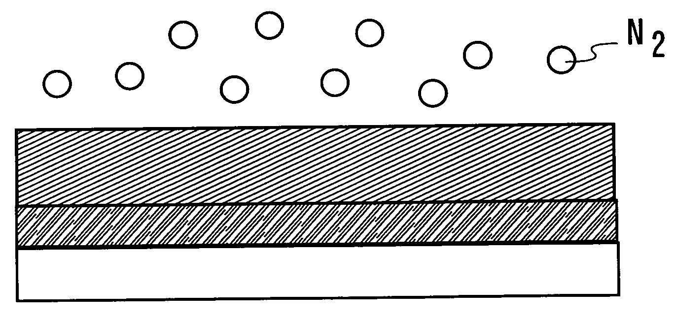
[0009] Accordingly, it is an object of the present invention to improve reliability of a light emitting device having a mixed layer including an organic compound and metaloxide without reducing productivity. The present invention solves the above described problem in such a way that after forming a mixed layer including an organic compound and metal oxide, the mixed layer is exposed to a nitrogen (N2) gas atmosphere without being exposed to a gas atmosphere including oxygen, and then a stacked film is formed without exposing the mixed layer to a gas atmosphere including oxygen. The gas atmosphere including oxygen indicates a gas atmosphere including an oxygen atom such as oxygen gas, NO2 gas, N2O gas or the like. After the formation of the mixed layer including the organic compound and metal oxide, by exposing the mixed layer to the nitrogen (N2) gas atmosphere without being exposed to a gas atmosphere including oxygen, film quality and reliability are improved without reducing productivity.
[0058] When after forming a mixed layer, the mixed layer is exposed to a nitrogen gas atmosphere without being exposed to a gas atmosphere including oxygen and a subsequent stacked film is formed without exposing the mixed layer to a gas atmosphere including oxygen, life of light emitting luminance can be improved without reducing productivity and deteriorating a characteristic of a light emitting device.
Problems solved by technology
However, there has been a problem of shortening luminance half life in the above described structures (patent document 2).
Method used
Image
Click on the blue label to locate the original text in one second.
Reading with bidirectional positioning of images and text.
Examples
embodiment modes
[0082] The embodiment modes of the present invention will be described below with reference to the accompanying drawings. It is easily understood by those skilled in the art that the embodiment modes and details herein disclosed can be modified in various ways without departing from the purpose and the scope of the invention. The present invention should not be interpreted as being limited to the description of the embodiment modes to be given below.
embodiment mode 1
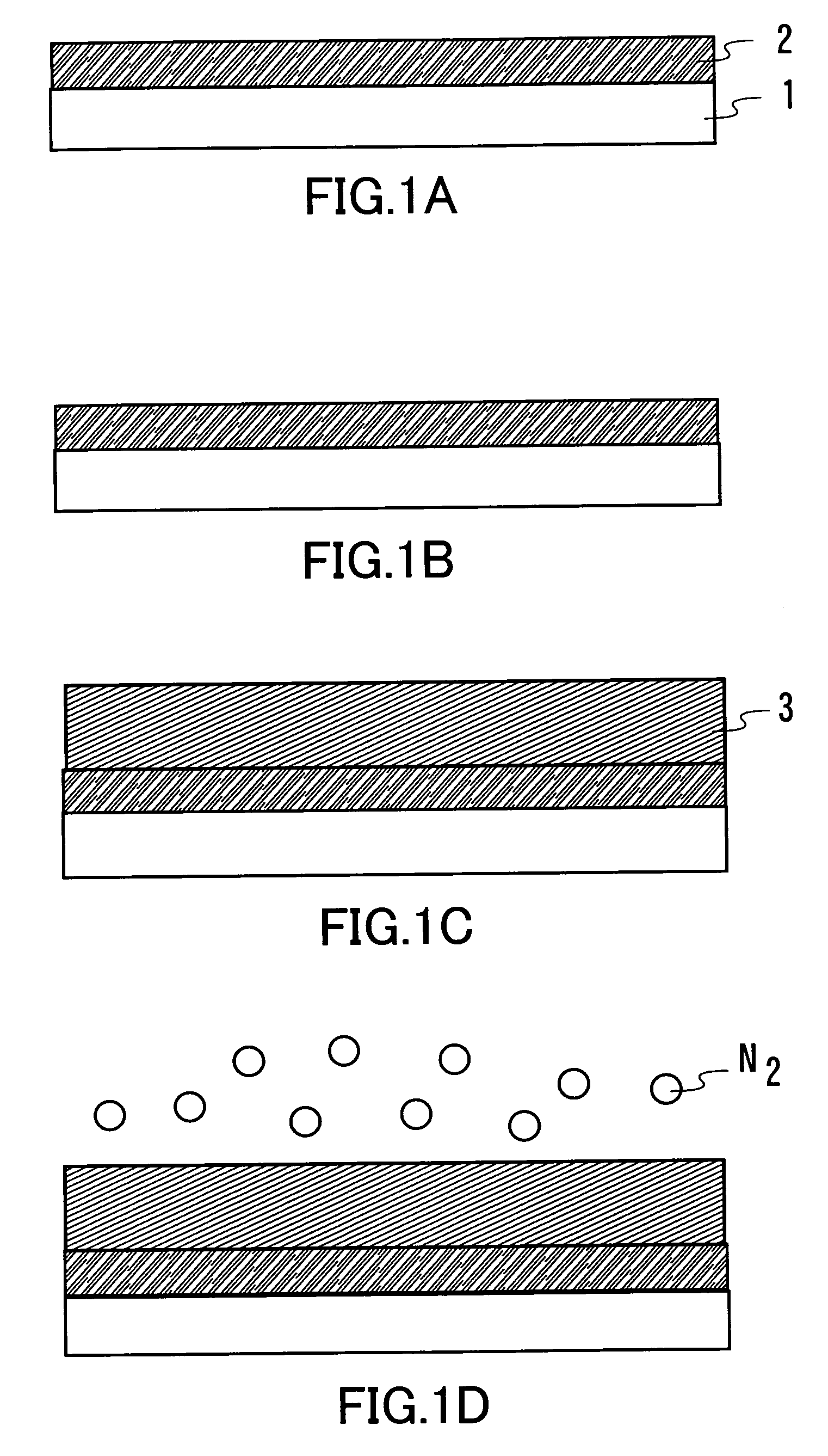
[0083] In a method for manufacturing a light emitting device including an anode, a cathode, a light emitting layer provided between the anode and the cathode, and a mixed layer including an organic compound and metal oxide provided between the anode and the light emitting layer, this embodiment mode will explain treatment in which the mixed layer is exposed to a nitrogen gas atmosphere after formation of the mixed layer.
[0084] An anode 2 is formed over a substrate 1 to have a thickness of 10 to 1,000 nm (FIG. 1A). As the substrate 1, quartz, glass, plastic, or the like can be used, for example. Further, other material may be used as the substrate 1 so long as it can serve as a supporting body in a process of manufacturing the light emitting device.
[0085] The anode 2 has a function of injecting holes to the light emitting layer. The anode 2 can be formed by using various kinds of metal; an alloy; an electroconductive compound; or a metal mixture thereof. For example, metal having a...
embodiment mode 2
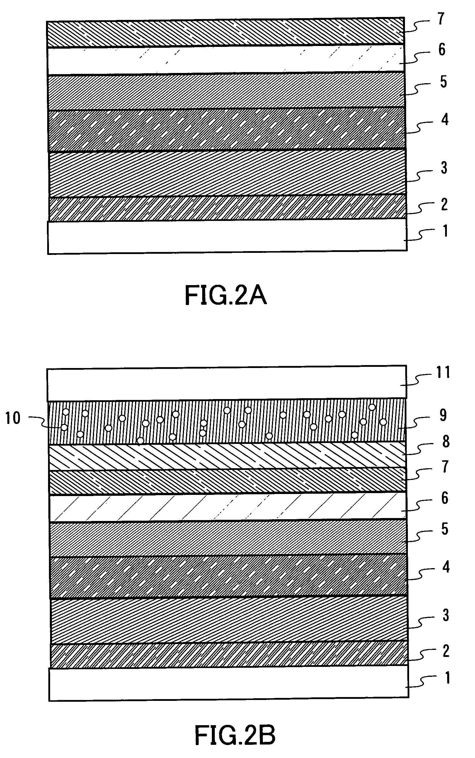
[0121] In this embodiment mode, a structure different from the structure shown in Embodiment Mode 1 will be described. In the structure shown in this embodiment mode, the mixed layer 3 is provided to be in contact with the cathode.
[0122]FIG. 3A shows one example of a structure of a light emitting device. In FIG. 3A, the hole transporting layer 4, the light emitting layer 5, the electron transporting layer 6, a first layer 15, the mixed layer 3 are stacked between the anode 2 and the cathode 7. The anode 2, the cathode 7, the hole transporting layer 4, the light emitting layer 5, the electron transporting layer 6, and the mixed layer 3 shown in Embodiment Mode 1 can be used in this embodiment mode.
[0123] The first layer 15 is an electron injecting layer and contains a substance having an electron donating property and a substance having an electron transporting property. As the substance having the electron donating property contained in the first layer 15, alkali metal, alkali ear...
BACKGROUND OF THE INVENTION [0001] 1. Field of the Invention [0002] The present invention relates to a method for manufacturing an electroluminescencelight emitting device used for a planar light source or a display element (hereinafter, also referred to as a “light emitting device”). [0003] 2. Description of the Related Art [0004] An electroluminescence light emitting device has a light emitting layer formed using an organic compound and the like. Such an electroluminescence light emitting device is attracting attention for realizing a large-area display element at low driving voltage. [0005] To improve efficiency of an element, Tang et al. proposed a structure in which organic compounds having different carrier transporting properties are stacked to inject holes and electrons from an anodeelectrode layer and a cathodeelectrode layer with good balance. Further, a thickness of an organic layer is set to be 200 nm or less to realize light emitting luminance of 1,000 cd / m2 and exte...
Claims
Application Information
Patent Timeline
Application Date:The date an application was filed.
Publication Date:The date a patent or application was officially published.
First Publication Date:The earliest publication date of a patent with the same application number.
Issue Date:Publication date of the patent grant document.
PCT Entry Date:The Entry date of PCT National Phase.
Estimated Expiry Date:The statutory expiry date of a patent right according to the Patent Law, and it is the longest term of protection that the patent right can achieve without the termination of the patent right due to other reasons(Term extension factor has been taken into account ).
Invalid Date:Actual expiry date is based on effective date or publication date of legal transaction data of invalid patent.

