Memory element, memory read-out element and memory cell

a memory element and read-out element technology, applied in the field of non-volatile storage using resistance elements, can solve the problems of limited scaling potential, large area usage, and lock cells, and achieve the effect of allowing only a limited number of write cycles, and limited scaling potential

Inactive Publication Date: 2007-01-04
POLARIS INNOVATIONS
View PDF6 Cites 41 Cited by
  • Summary
  • Abstract
  • Description
  • Claims
  • Application Information

AI Technical Summary

Benefits of technology

[0018] One object of the invention is to provide an efficient concept for writing to and reading from memory elements having resistance el

Problems solved by technology

What may be disadvantageous about the SRAM cells and the latch cells may be that they are volatile and have a considerable area usage.
Flash technology is furthermore distinguished by an only limited scaling potential and permits only a limited number of write cycles.
What may be disadvantageous about the above concept may be inflexibility in the write operation.
Consequently, the amplitudes of the currents depend on one another, so that it is not possible for them to be set precisely and individually.
Furthermore, different voltages have to be generated across the resistance elements, which is associated with a high outlay.
High losses (leakage) furthermore arise because the PCM elements attain a resistance value in the region of 1 MΩ in the high-resistance state.
Such a current loss (leakage current) may be unacceptable for some applications.
A further possible disadvantage of the above concept may be that there is a risk of a destructive read-out during the read-out of the memory cells.
What may be disadvantageous about the above cell is that the read-out may be susceptible to errors.
What may furthermore be disadvantageous is that a destructive read out of the PCM elements involving the erasure of the stored information during read-out may, in some cases, only be prevented by means of a precise voltage ramp on the “PL” line.
This may increase the production costs because components having smaller tolerances may have to be provided for this purpose.
Moreover, on account of the precise control which may be used in order to avoid the read-out errors, the control outlay may be increased,

Method used


Image

  • Memory element, memory read-out element and memory cell
  • Memory element, memory read-out element and memory cell
  • Memory element, memory read-out element and memory cell

Examples


Embodiment Construction

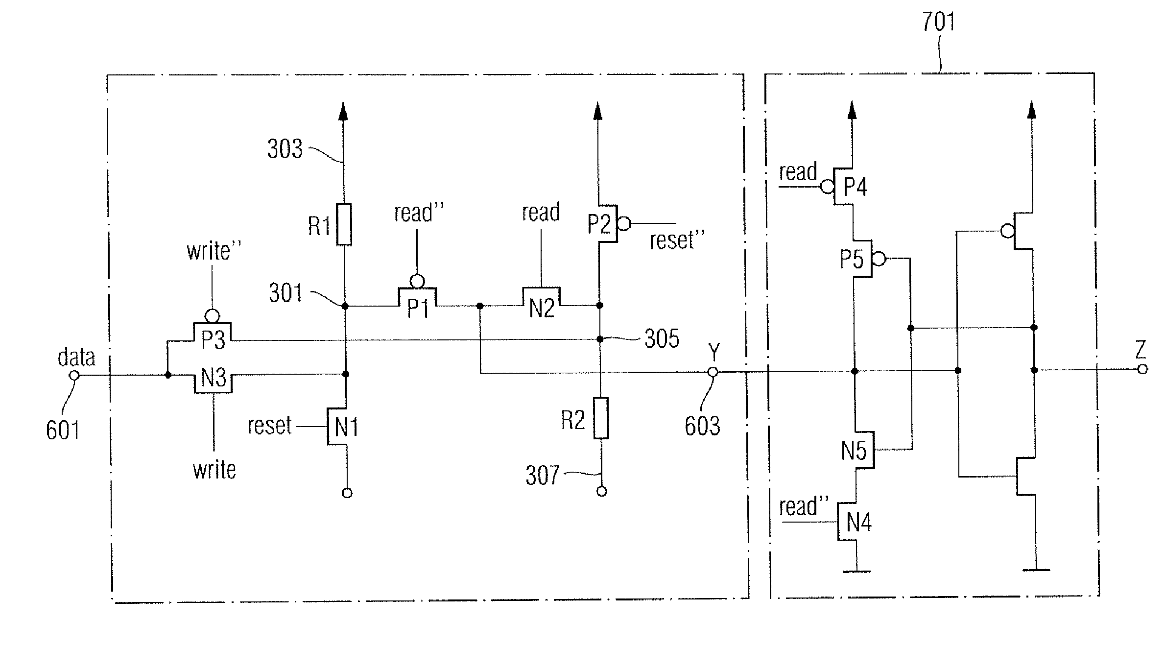
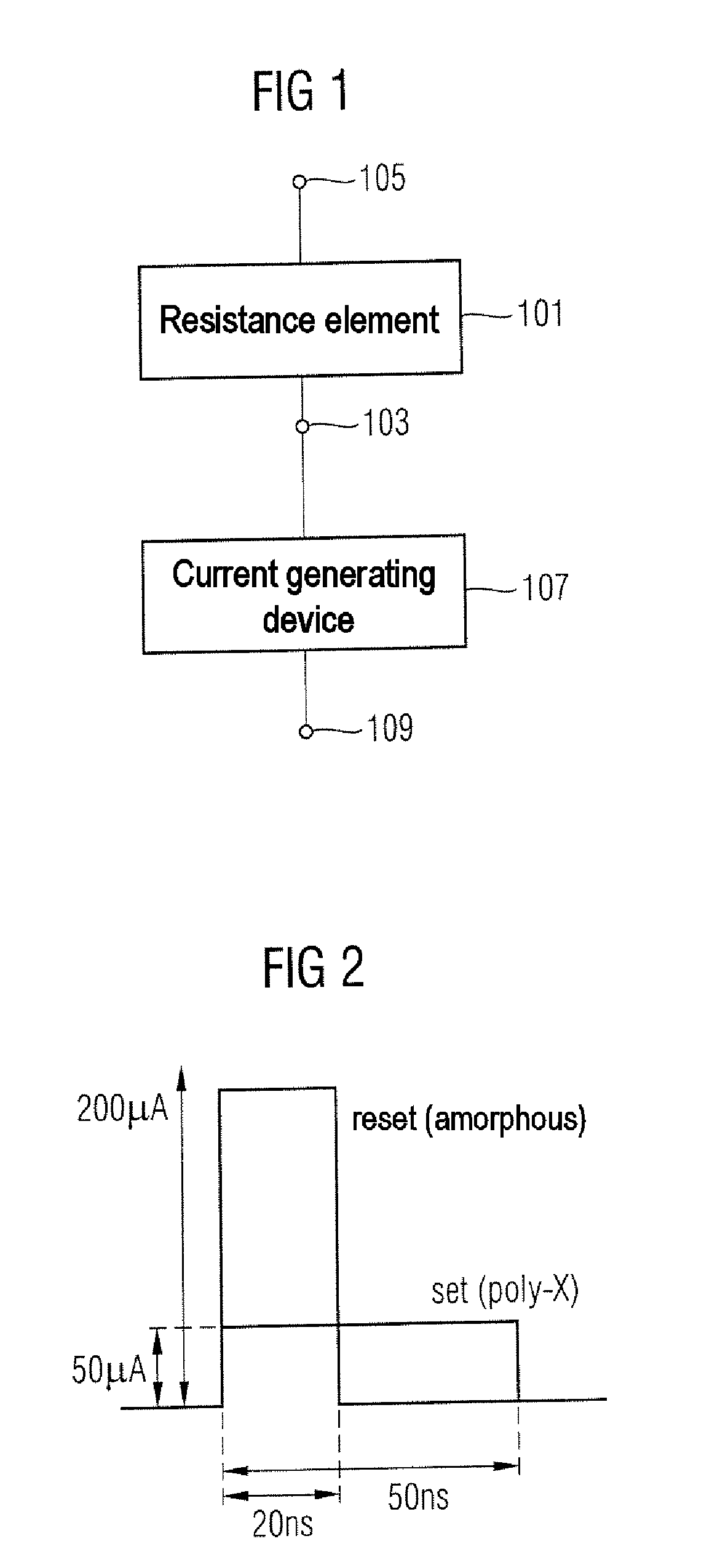
[0046] In one embodiment, the memory element illustrated in FIG. 1 comprises a resistance element 101 having a first terminal 103 and a second terminal 105. The memory element furthermore comprises a current generating device 107, the output of which is coupled, for example, electrically connected, to the first terminal 103 of the resistance element 101.

[0047] The current generating device 107 may furthermore comprise a terminal 109, to which a reference potential, for example, an earth potential, can be applied.

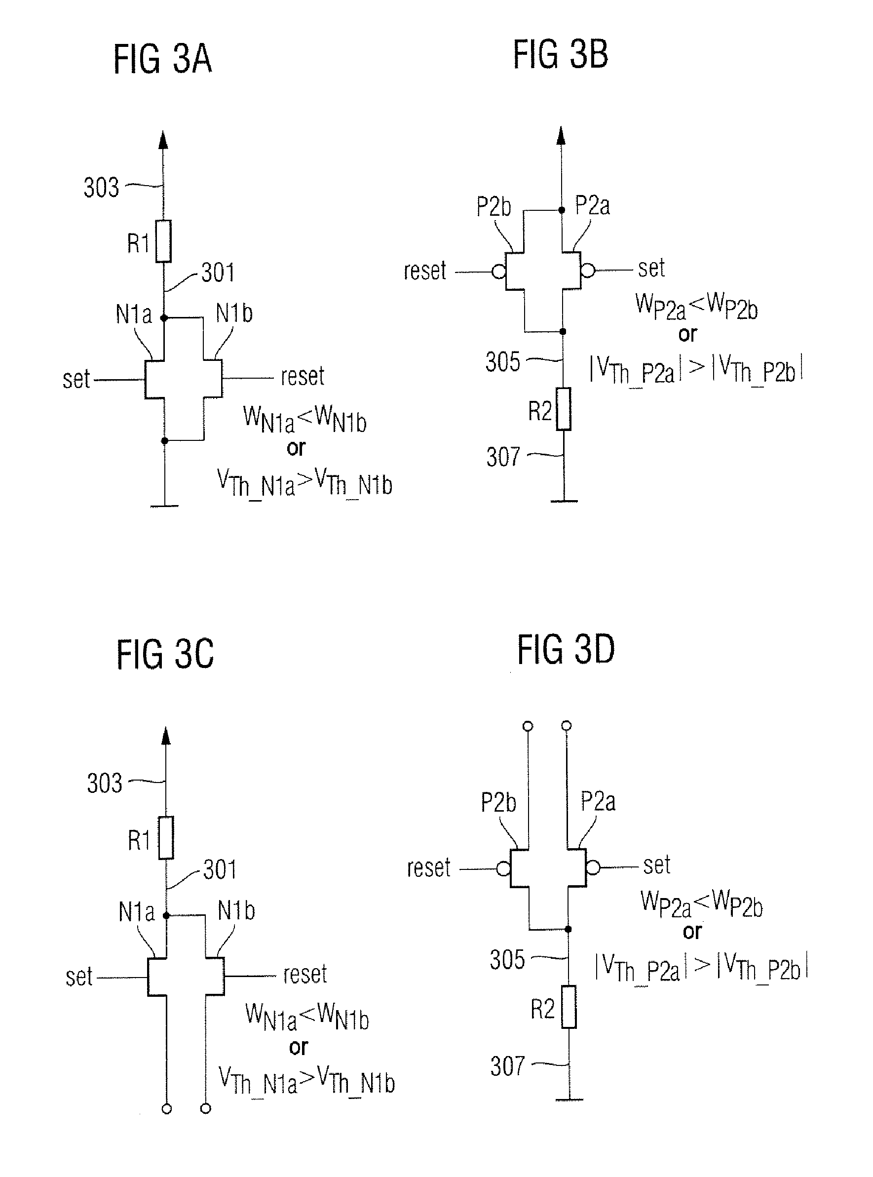
[0048] The resistance element 101 has a first resistance value in a first state and a second resistance value in a second state, the two resistance values being different from one another. Furthermore, the states are reversible so that the resistance element 101 can be converted both from the first state into the second state and from the second state into the first state. The resistance element 101 may be a PCM element, for example, in which the first state is an amorphou...


PUM


Abstract

A memory element comprises a resistance element having a first resistance value in a first state and a second resistance value in a second state, it being possible to convert the resistance element from the first state into the second state and from the second state into the first state and the first resistance value and the second resistance value being different, a current generating device, coupled to a first terminal of the resistance element, the current generating device being designed to generate a current with a first amplitude through the resistance element when a predetermined potential is present at a second terminal of the resistance element, in order to convert the resistance element into the first state for setting the first resistance value, or to generate a current with a second amplitude through the resistance element when the predetermined potential is present at the second terminal of the resistance element, in order to convert the resistance element into the second state for setting the second resistance value, the first resistance value representing a first memory state and the second resistance value representing a second memory state.

Description

CROSS-REFERENCE TO RELATED APPLICATIONS [0001] This application claims foreign priority benefits under 35 U.S.C. §119 to co-pending German patent application number 10 2005 030 143.6, filed Jun. 28, 2005. This related patent application is herein incorporated by reference in its entirety. BACKGROUND OF THE INVENTION [0002] 1. Field of the Invention [0003] Embodiments of the invention relate to non-volatile storage using resistance elements, in particular, using phase change memory elements (PCM). [0004] 2. Description of the Related Art [0005] Memory cells may be used in all applications which use data storage. Typical semiconductor circuits comprise data memory cells which are either formed between logic elements, such as, e.g., latch registers, or which are formed as block memories, such as SRAM (static random access memory), for example. A block memory typically comprises an array of memory cells, only a few cells being subjected to a write operation or a read-out operation simul...

Claims


Application Information

Patent Timeline
IPC IPC(8): G11C11/34
CPCG11C13/0004G11C13/003G11C2213/74G11C13/0069G11C2013/0071G11C13/004
Inventor SCHOENAUER, TIMKUND, MICHAELNIEDERMEIER, THOMASBERTHOLD, JOERG
Owner POLARIS INNOVATIONS
Why Eureka
Try Eureka