
Small, scalable resistive element and method of manufacturing

Inactive Publication Date: 2005-01-20
IBM CORP +1
View PDF1 Cites 0 Cited by
  • Summary
  • Abstract
  • Description
  • Claims
  • Application Information

AI Technical Summary

Benefits of technology

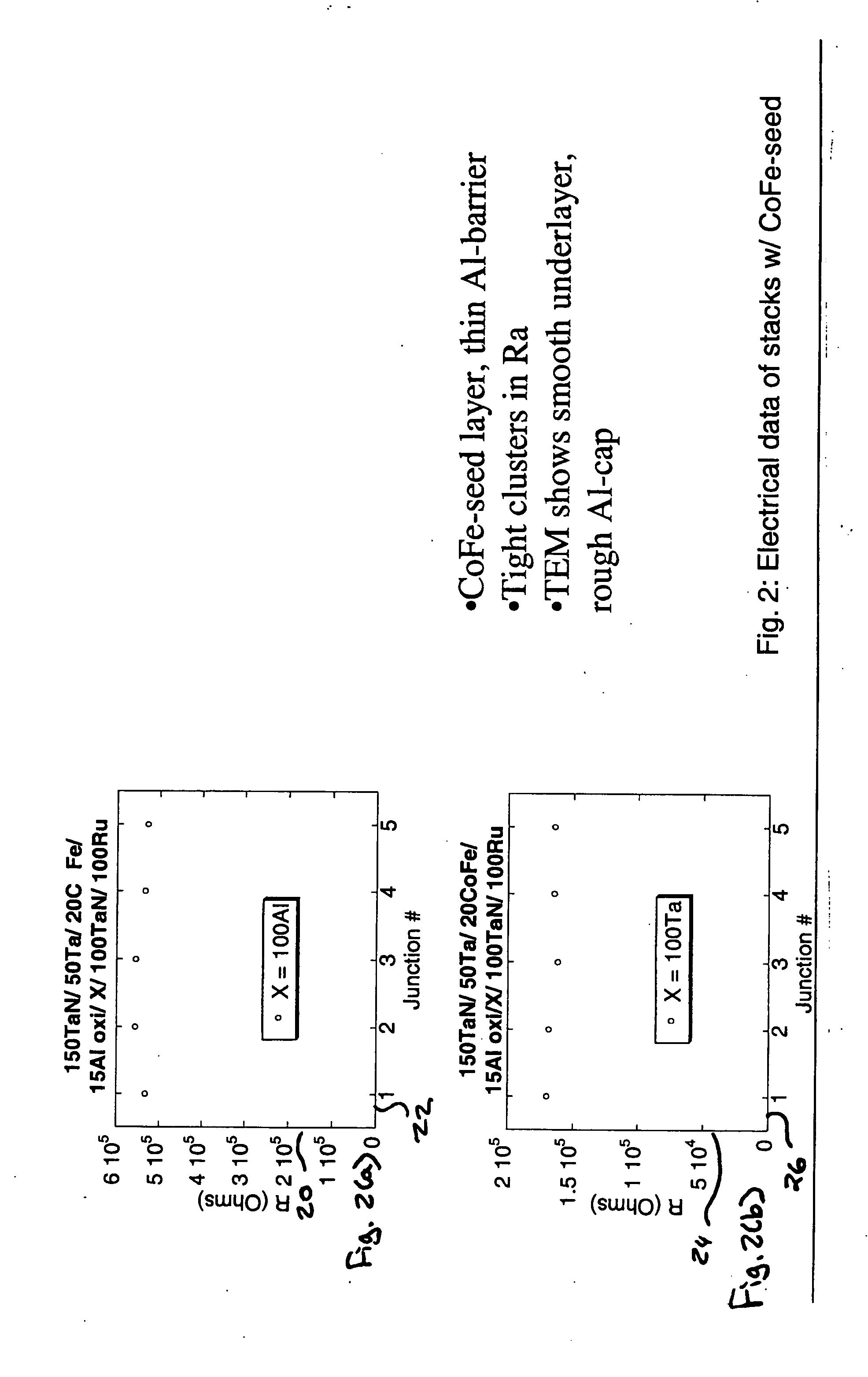
[0007] The above described preferred embodiments of the present invention represent a number of improvements upon the prior art. First, unlike prior art resistors, resistors can be constructed in accordance with the present invention to have both a small feature size (because of the vertical structure of the resistor) and a large resistance value. Second, the present invention provides resistors that can reliably be constructed to have a particular resistance value with very little variance in their resistance values. Finally, the resistance value of the resistors can be easily modified by patterning them to have a particular resistance value during an etching process already typically present during the manufacturing process. As an option, the resistance value can also be set by a proper choice of Al thickness and appropriate barrier oxidation. Thus, the present invention represents a substantial improvement upon the prior art.

Problems solved by technology

However, as integrated circuits increasingly become more complex with more components, they require more and more space on semiconductor substrates to construct.

Method used


Image

  • Small, scalable resistive element and method of manufacturing
  • Small, scalable resistive element and method of manufacturing
  • Small, scalable resistive element and method of manufacturing

Examples


Embodiment Construction

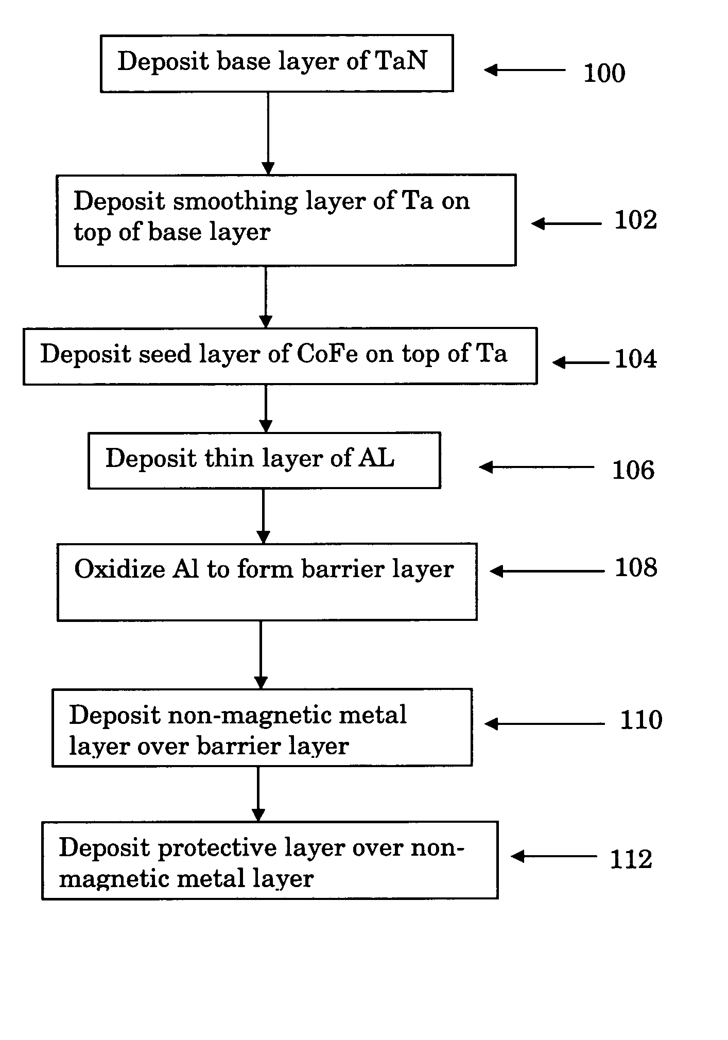
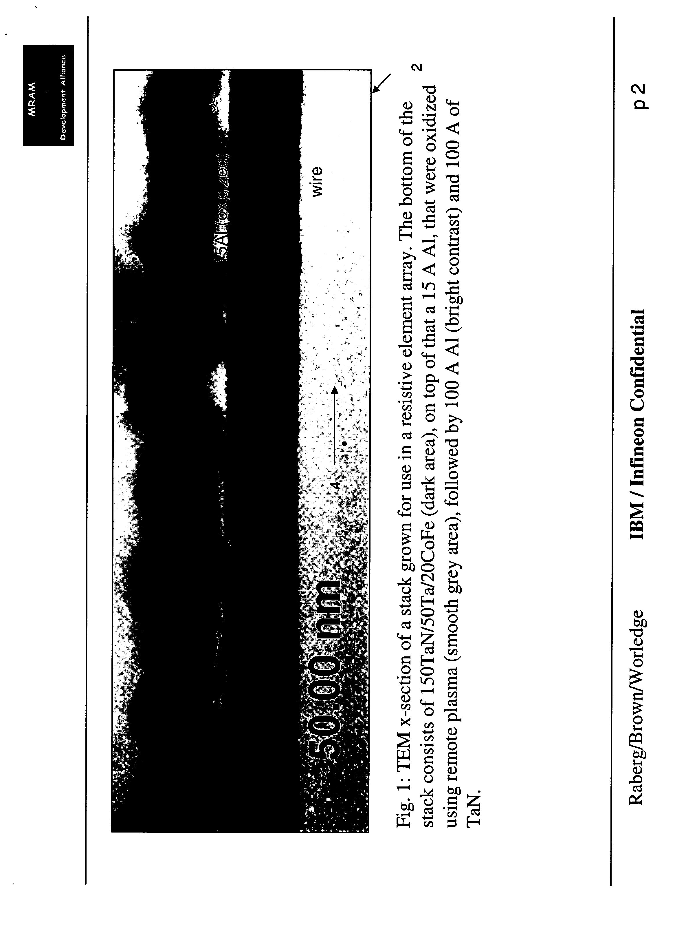
[0012] Referring now to FIG. 1, a representation of a resistive stack 2 manufactured in accordance with a preferred embodiment of the present invention is shown. A picture of a resistive stack such as shown in FIG. 1 may be obtained in practice by viewing the resistive stack with a transition electron microscope (TEM). The resistive stack 2 is constructed upon a metal line or layer 4. As discussed in more detail below, the metal line 4 provides one electrical contact point to the resistive stack 2. A Tantalum Nitride (TaN) layer 6 is deposited upon the metal layer 4 to form a base layer 6 of the resistive stack 2. The TaN layer 6 is depicted in FIG. 1 as being 150 Angstroms (A) thick. However, the thickness of the base layer 6 is not critical as long as it does not deviate to the point that the functionality of the resistive stack 2 is substantially affected. In order to provide a smoother surface for deposition of a seed layer, a thin smoothing layer of Tantalum (Ta) 8 is deposited...


PUM


Abstract

An improved scalable, resistive element for use in a semiconductor device that can be produced with a small feature size and precise resistance is provided by the present invention. The resistive element includes a base layer positioned on top of a metal line. A seed layer of is deposited on top of the base layer. A thin barrier layer of Al is deposited on top of the seed layer and oxidized. A non-magnetic metal layer is then deposited on top of the barrier layer. The base layer and the non-magnetic metal layer form electrodes on either side of the barrier layer. The barrier layer is thin enough that a tunneling current can travel between the electrodes. The resulting resistive element may be constructed with a high resistance and a very small feature size.

Description

FIELD OF THE INVENTION [0001] This invention generally relates to the field of semiconductor manufacturing. More particularly, the present invention disclosure describes an improved process for manufacturing resistive elements that are smaller than conventional resistors and well suited for integration into modern semiconductor devices. BACKGROUND OF THE INVENTION [0002] Resistors are a basic electrical component of almost every integrated circuit. Modern integrated circuits are typically manufactured from semiconductors using a process whereby layers of materials are deposited upon a semiconductor substrate and then patterned by selectively etching away portions of the deposited layers. Typically, resistors are formed by depositing a length of conductive material having a predetermined resistance per unit of length such that the length of the resistor determines its particular resistance value. Thus, to create a resistor having a relatively high resistance, a relatively long length...

Claims


Application Information

Patent Timeline
IPC IPC(8): H01C7/00H01L21/02H01L27/08
CPCH01C7/006H01L28/24H01L27/0802
Inventor WORLEDGE, DANIELKLOSTERMANN, ULRICHRABERG, WOLFGANGBROWN, STEPHEN L.
Owner IBM CORP
Learn More