Mask pattern for semiconductor device fabrication, method of forming the same, and method of fabricating finely patterned semiconductor device

a semiconductor device and mask pattern technology, applied in the field of mask pattern for fabricating semiconductor devices, can solve the problems of material-dependent and uneconomical, short-wavelength exposure tool based lithography, material-dependent and uneconomical, etc., and achieve the effect of reducing the width of the opening

Inactive Publication Date: 2005-10-13
SAMSUNG ELECTRONICS CO LTD
View PDF8 Cites 24 Cited by
  • Summary
  • Abstract
  • Description
  • Claims
  • Application Information

AI Technical Summary

Benefits of technology

[0015] The present disclosure also provides a method of forming a mask pattern for semiconductor device fabrication, which can be used in forming a fine pattern with a smaller feature size while minimizing the transformation of the sidewall profile of openings or spaces.
[0016] The present disclosure also provides a method of fabricating a semiconductor device, which can form a fine pattern above the wavelength limit of lithography while minimizing the transformation in the sidewall profile of openings or spaces.
[0032] According to the present disclosure, in formation of a mask pattern used as an etching mask of an underlayer, a self-assembled molecular monolayer is selectively formed only on a surface of a resist pattern in a self-assembled manner. Therefore, the mask pattern can have small-sized openings above the wavelength limit established by lithography. Furthermore, since the self-assembled molecular monolayer can be repeatedly formed on the surface of the resist pattern, the openings of the mask pattern can be reduced to desired width. Still furthermore, the width reduction of the openings can be performed by a simple method at room temperature, instead of thermal treatment.

Problems solved by technology

The short-wavelength exposure tool based lithography has many difficulties in that it is material-dependent and uneconomical.
The half-tone phase shift mask based lithography has limitations on mask formation technology and resolution, and thus, it is very difficult to form contact holes which are less than 150 nm in size.
Therefore, this technology has a limitation in adjusting the flow rate of the resist pattern, which makes it difficult to reduce the CD of the resist pattern while maintaining a vertical profile shape.
However, polyvinylalcohol used as the resin in this method has a high viscosity and is water-insoluble, and thus, it is difficult to completely remove the resin by rinsing with deionized water.
However, chemical crosslinking reaction may also occur at an unwanted position, thereby causing pattern defects.
However, since the amount of thermal shrinkage in the coating agent mainly depends on the temperature profile of the substrate, it is difficult to form uniform resist patterns on the whole surface of the substrate.
As described above, among CD reduction technologies that have been suggested hitherto, a resist flow technology by thermal treatment cannot provide a good sidewall profile.
Coating of a separate material on a resist pattern may induce an unwanted crosslinkage in the resist pattern, thereby causing pattern defects.
Furthermore, the material remained on an unwanted region may cause pattern defects or “not open” of holes.
These problems may worsen as the sizes of holes or trenches to be formed decrease.

Method used


Image

  • Mask pattern for semiconductor device fabrication, method of forming the same, and method of fabricating finely patterned semiconductor device
  • Mask pattern for semiconductor device fabrication, method of forming the same, and method of fabricating finely patterned semiconductor device
  • Mask pattern for semiconductor device fabrication, method of forming the same, and method of fabricating finely patterned semiconductor device

Examples


example 1

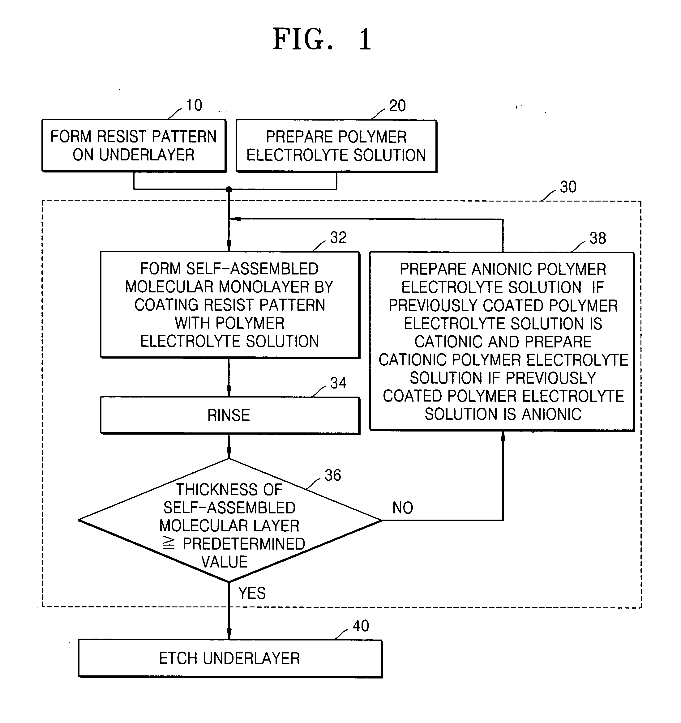
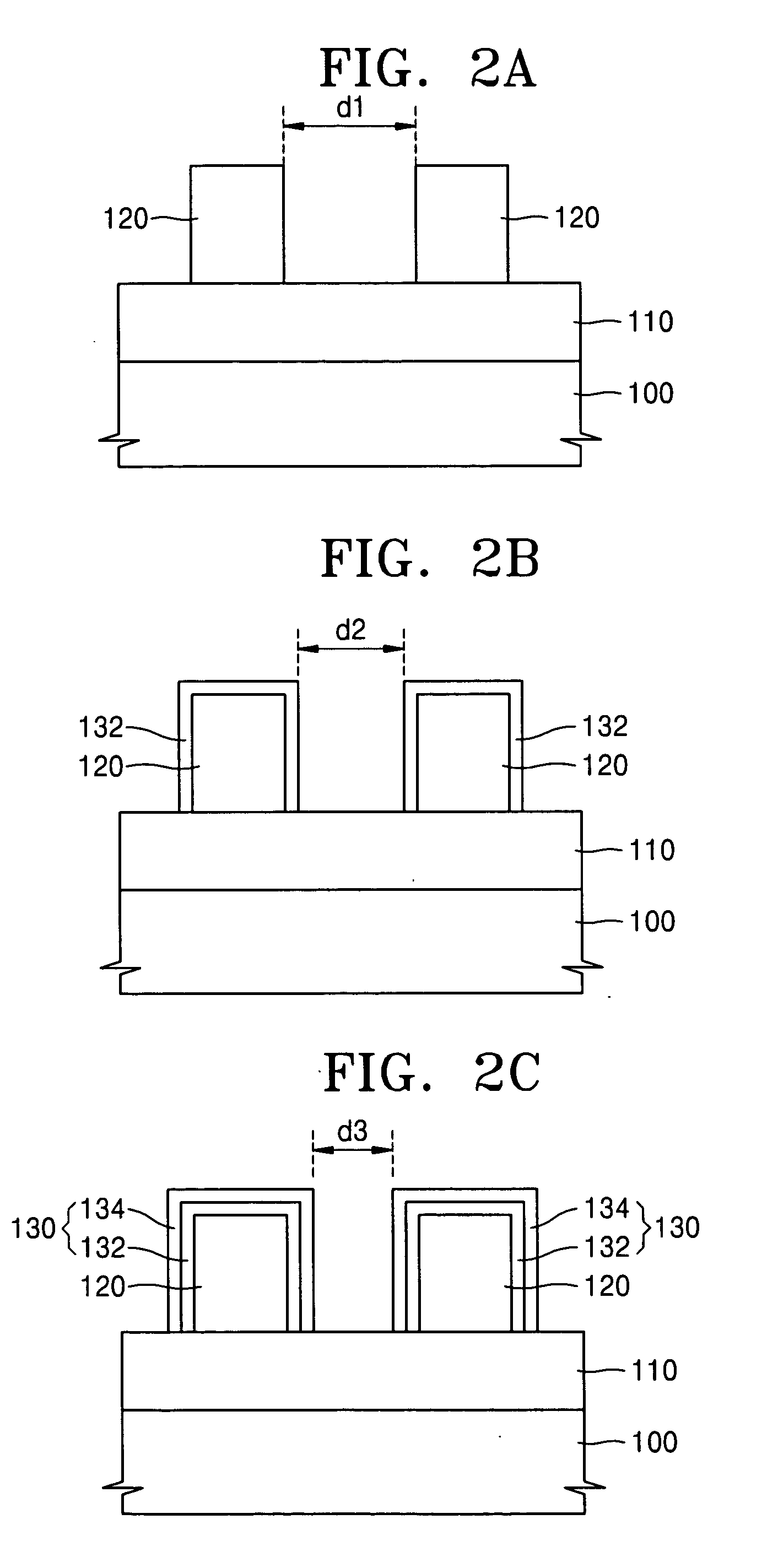
[0078] An organic antireflective film (DUV-30, Nissan Chemical Industries, Ltd.) was formed to a thickness of 36 nm on a bare silicon wafer and a photoresist (SAIL-G24c, ShinEtsu Chemical Co. Ltd) was coated thereon to form a resist film with a thickness of 240 nm. The wafer, on which the resist film was formed, was subjected to soft baking, followed by exposure with ArF (193 nm) stepper (Nikon S306C) specified with numeric aperture (NA) of 0.75 (annular illumination: 0.85-0.55) and 24 mJ / cm2 exposure light energy, and post-exposure baking (PEB). Then, the wafer was developed with a 2.38 wt % tetramethylammonium hydroxide (TMAH) solution to form, on the wafer, a resist pattern with openings having a CD (critical dimension) of 116.8 nm.

[0079] 3 ml of an aqueous solution of 1,000 ppm branched polyethyleneimine used as a cationic polymer electrolyte solution was spin-coated on the resist pattern at 1,000 rpm for about 30 seconds to obtain a mask pattern with openings having a smaller ...

example 2

[0081] A mask pattern with openings having a CD of 103.4 nm was formed in the same manner in Example 1 except that an aqueous solution of 5,000 ppm branched polyethyleneimine was used as the cationic polymer electrolyte solution.

example 3

[0082] A resist pattern with a CD of 116.8 nm was formed on a wafer in the same manner as in Example 1. Then, 3 ml of an aqueous solution of 1,000 ppm branched polyethyleneimine used as a cationic polymer electrolyte solution was spin-coated on the resist pattern at 1,000 rpm for about 30 seconds and then rinsed with deionized water.

[0083] 3 ml of an aqueous solution of 1,000 ppm poly(styrene-4-sulfonate) used as an anionic polymer electrolyte solution was spin-coated at 1,000 rpm for about 30 seconds and then rinsed with deionized water to obtain a mask pattern with openings having a smaller CD of 106.1 nm.

[0084] 3 ml of an aqueous solution of 1,000 ppm poly(diallydimethyl ammonium chloride) used as a cationic polymer electrolyte solution was spin-coated on the mask pattern at 1,000 rpm for about 30 seconds and then rinsed with deionized water.

[0085] 3 ml of an aqueous solution of 1,000 ppm poly(styrene-4-sulfonate) used as an anionic polymer electrolyte solution was spin-coated...


PUM

PropertyMeasurementUnit
temperatureaaaaaaaaaa
sizeaaaaaaaaaa
timeaaaaaaaaaa

Abstract

Provided are a mask pattern including a self-assembled molecular layer, a method of forming the same, and a method of fabricating a semiconductor device. The mask pattern includes a resist pattern formed on a semiconductor substrate and the self-assembled molecular layer formed on at least a sidewall of the resist pattern. To form the mask pattern, first, the resist pattern is formed with openings on an underlayer covering the substrate to expose the underlayer to a first width. Then, the self-assembled molecular layer is selectively formed on a surface of the resist pattern to expose the underlayer to a second width smaller than the first width. The underlayer is etched using the resist pattern and the self-assembled molecular layer as an etching mask to obtain a fine pattern.

Description

CROSS-REFERENCE TO RELATED APPLICATION [0001] This application claims priority under 35 U.S.C. §119 to Korean Patent Application No. 2004-24022, filed on Apr. 8, 2004, in the Korean Intellectual Property Office, the disclosure of which is incorporated by reference herein in its entirety. BACKGROUND OF THE INVENTION [0002] 1. Field of the Disclosure [0003] The present disclosure relates to semiconductor device fabrication. More particularly, the present disclosure relates to mask patterns for fabricating semiconductor devices, as well as methods of forming the same. [0004] 2. Description of the Related Art [0005] In a conventional patterning process for semiconductor device fabrication, after a photoresist pattern is formed on a predetermined film to be etched for pattern formation, such as, for example, on a silicon, dielectric, or conductive film, the predetermined film is etched by using the photoresist pattern as an etching mask to form a desired pattern. [0006] With the increase...

Claims


Application Information

Patent Timeline
Patent Type & Authority Applications(United States)
IPC IPC(8): G03F7/40G03F7/004G03F7/16H01L21/027H01L21/033H01L21/3065H01L21/308H01L21/311H01L21/3213
CPCB82Y30/00G03F7/165G03F7/40H01L21/0273H01L21/0337H01L21/32139H01L21/3081H01L21/3086H01L21/3088H01L21/31144H01L21/0338
Inventor HAH, JUNG-HWANKIM, HYUN-WOOYOON, JIN-YOUNGHATA, MITSUHIROSUBRAMANYA, KOLAKE MAYYAWOO, SANG-GYUN
Owner SAMSUNG ELECTRONICS CO LTD
Why Eureka
Try Eureka