

Wafer scale test interfact unit: low loss and high isolation devices and methods for high speed and high density mixed signal interconnects and contactors
a mixed signal and interfacial unit technology, applied in the field of mixed signal rf, high speed digital interconnects, shielded dc lines, can solve the problems of large test equipment, large noise, and tendency to smaller pitches, and achieve the effects of low loss, low loss, and low insertion loss
- Summary
- Abstract
- Description
- Claims
- Application Information
AI Technical Summary
Benefits of technology
Problems solved by technology
Method used
Image

Examples
Embodiment Construction
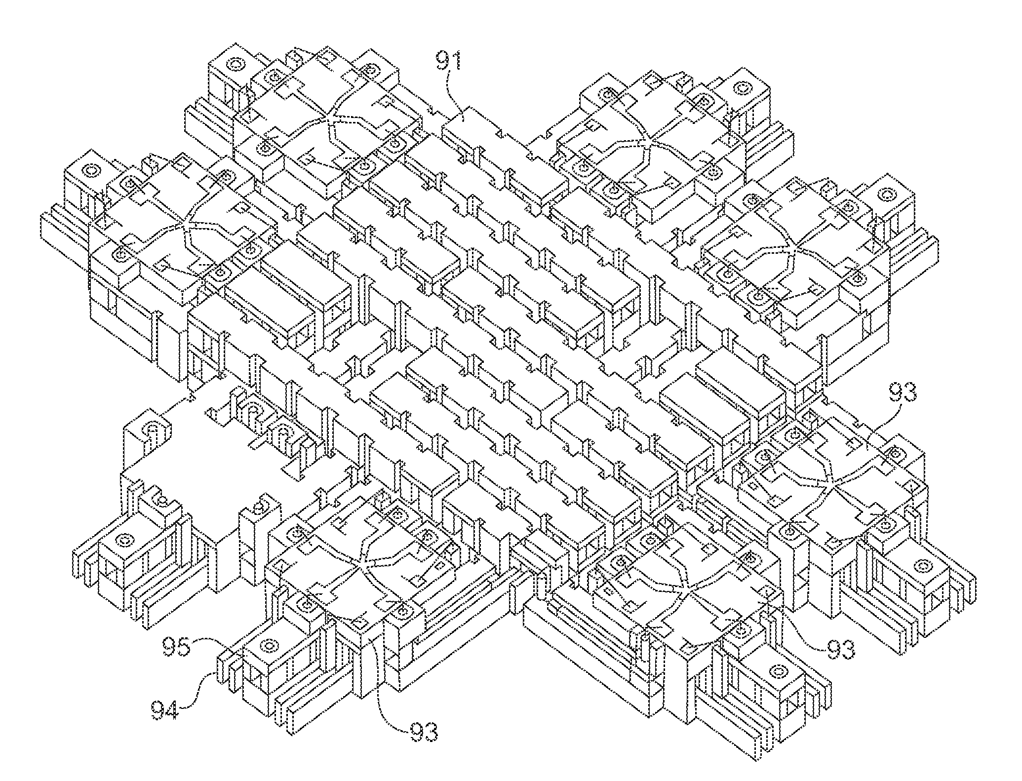
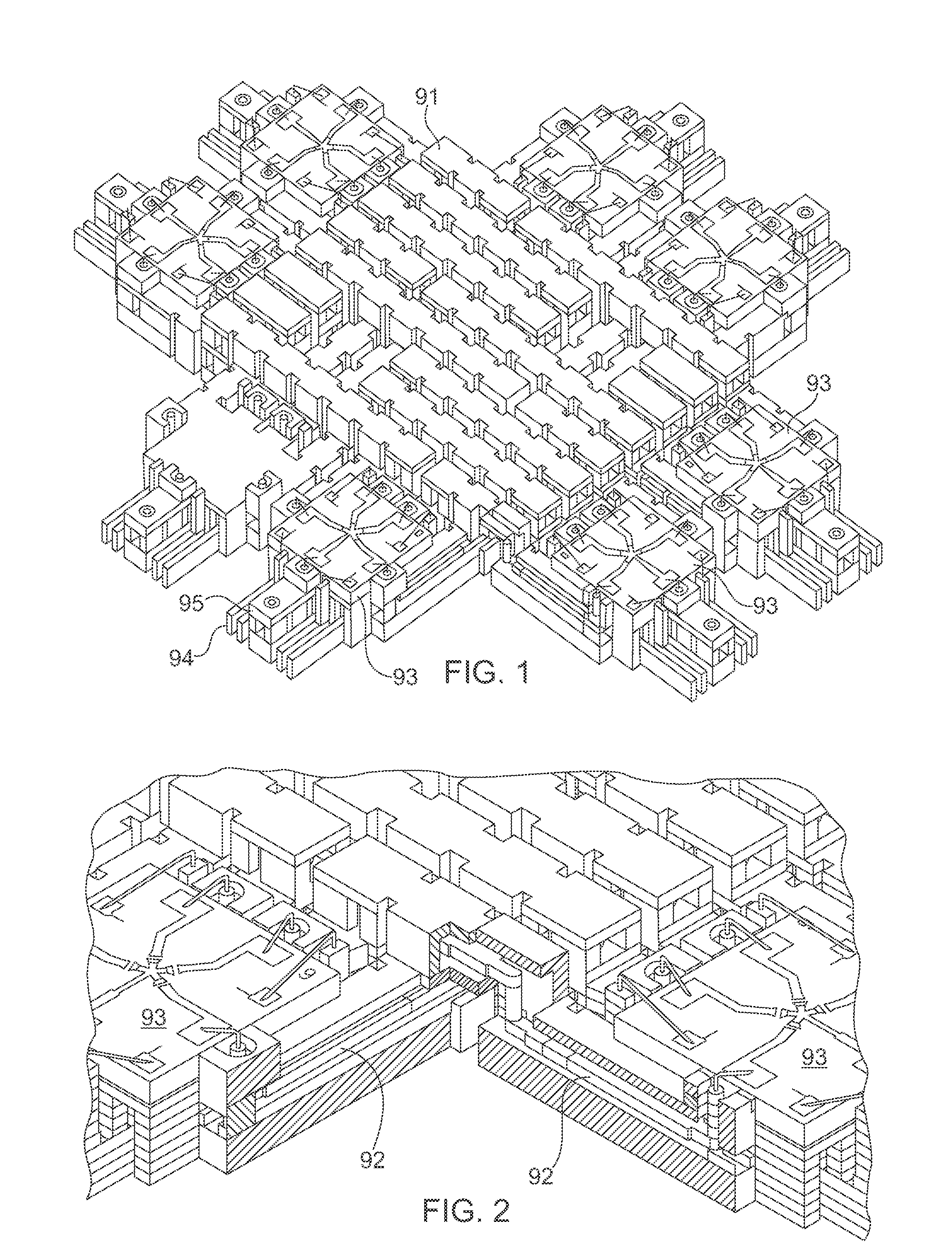
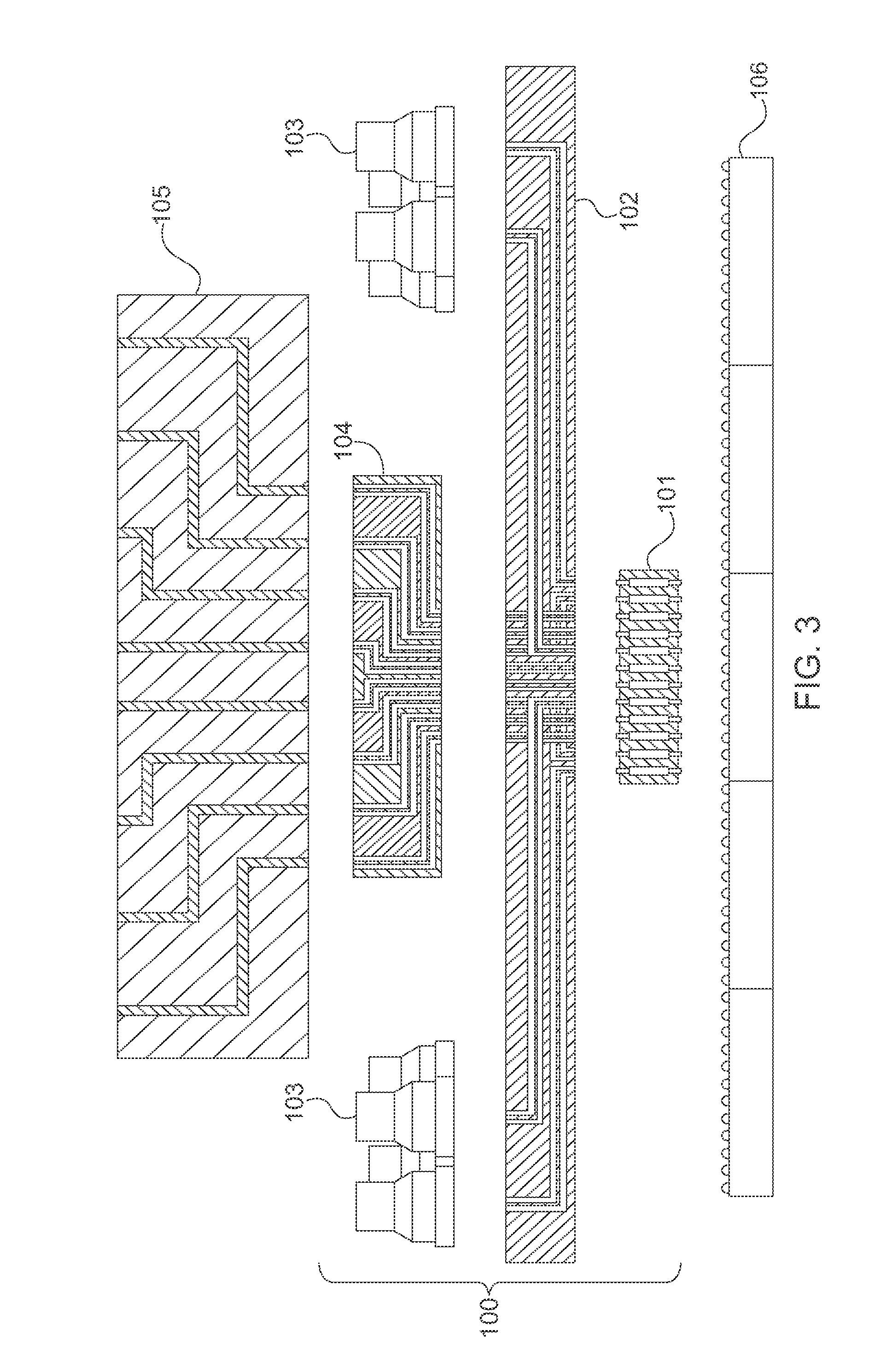
[0051]Referring now to the figures, wherein like elements are numbered alike throughout, FIGS. 3-4 schematically illustrate an exemplary configuration of a wafer level test interface unit 100 in accordance with the present invention for use in testing a device under test (DUT) 106. The wafer level test interface unit 100 may be configured to provide repeated testing of multiple devices under test 106, especially at the grid / wafer level, while overcoming numerous problems in the existing art. For example, typically, the device under test 106 will include RF and DC circuitry, which is typically tested through the use of a probe card assembly comprised of printed circuit boards 105 and a contactor array 101. (The printed circuit board 105 can represent a non-coaxial printed circuit card where processing or interfacing with active and passive components can be conducted close to the device under test 106.) However, the pitch of features on the device under test 106 is most often much fi...
PUM
 Abstract
Description
Claims
Application Information