Method of manufacturing piezoelectric vibrators

a piezoelectric vibrator and piezoelectric technology, applied in the direction of generator/motor, instrument, and semiconductor/solid-state device details, can solve the problems of uneven potential deformation corrosion of piezoelectric bonding material, etc., to achieve reliable anodic bonding, excellent energy efficiency, and excellent energy efficiency

Inactive Publication Date: 2014-12-02
SEIKO INSTR INC
View PDF11 Cites 0 Cited by
  • Summary
  • Abstract
  • Description
  • Claims
  • Application Information

AI Technical Summary

Benefits of technology

[0013]The present invention has been made in view of the foregoing, and an object of the present invention is to provide a method for manufacturing a package capable of achieving reliable anodic bonding between the bonding material and the board even when the bonding material having a large resistance value is used and to provide a method for manufacturing a piezoelectric vibrator.

Problems solved by technology

However, there is a problem in that when the bonding material used for the anodic bonding is exposed to the outside of the bonded package, the bonding material made of Al will be corroded, and airtightness of the package will be degraded.
As a result, there is a problem in that the potential of the bonding material will be uneven, and anodic bonding is not achieved at positions distant from the probe connection point although anodic bonding is achieved near the probe connection point.
In order to achieve the anodic bonding at positions distant from the probe connection point, it is necessary to perform anodic bonding by applying a high voltage, which may however increase the amount of energy consumption.
However, since the softening point of a glass board that forms the Si film is about 600° C., it is difficult to form the Si film on the glass board at a high temperature.

Method used


Image

  • Method of manufacturing piezoelectric vibrators
  • Method of manufacturing piezoelectric vibrators
  • Method of manufacturing piezoelectric vibrators

Examples


Embodiment Construction

Piezoelectric Vibrator

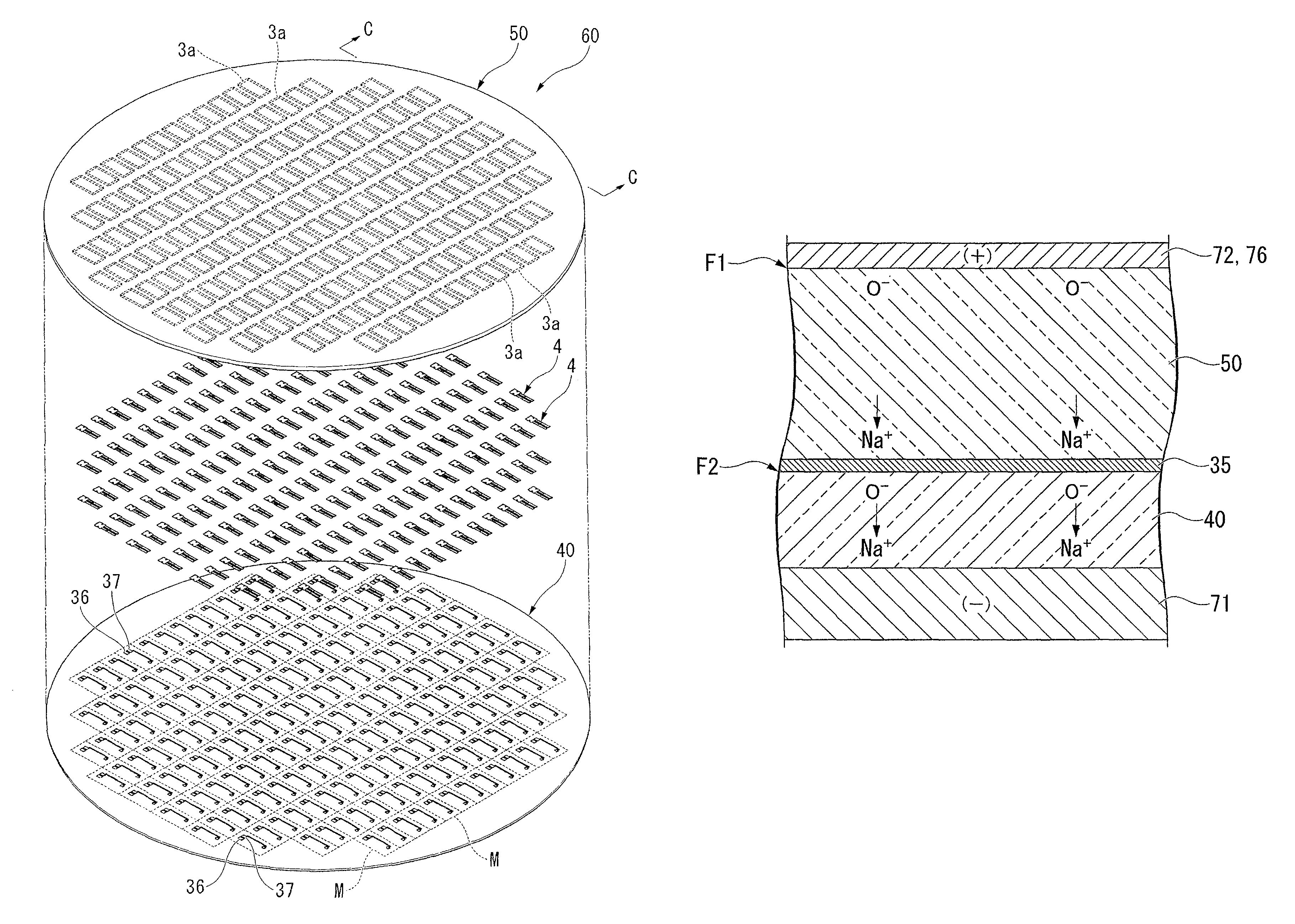
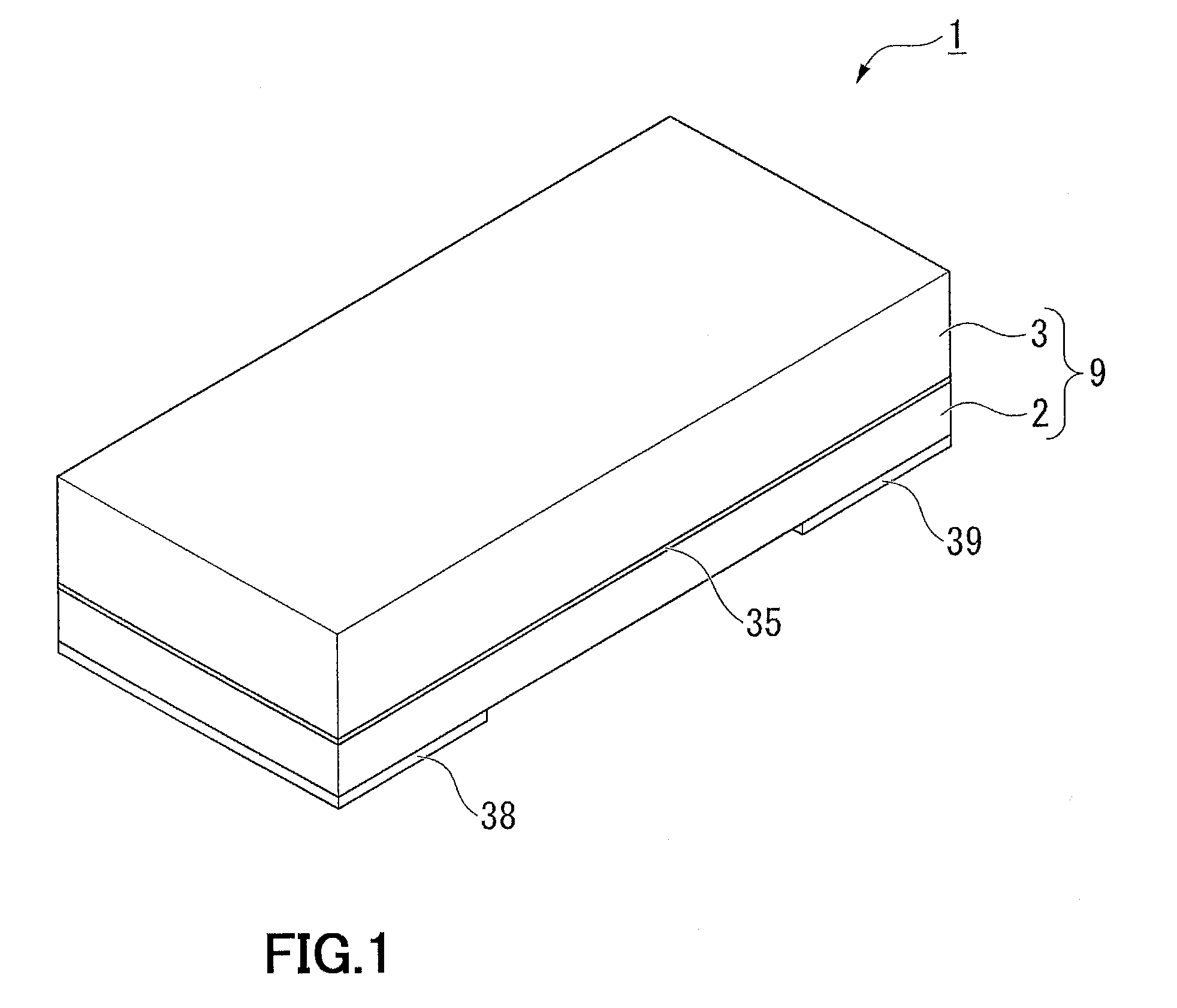
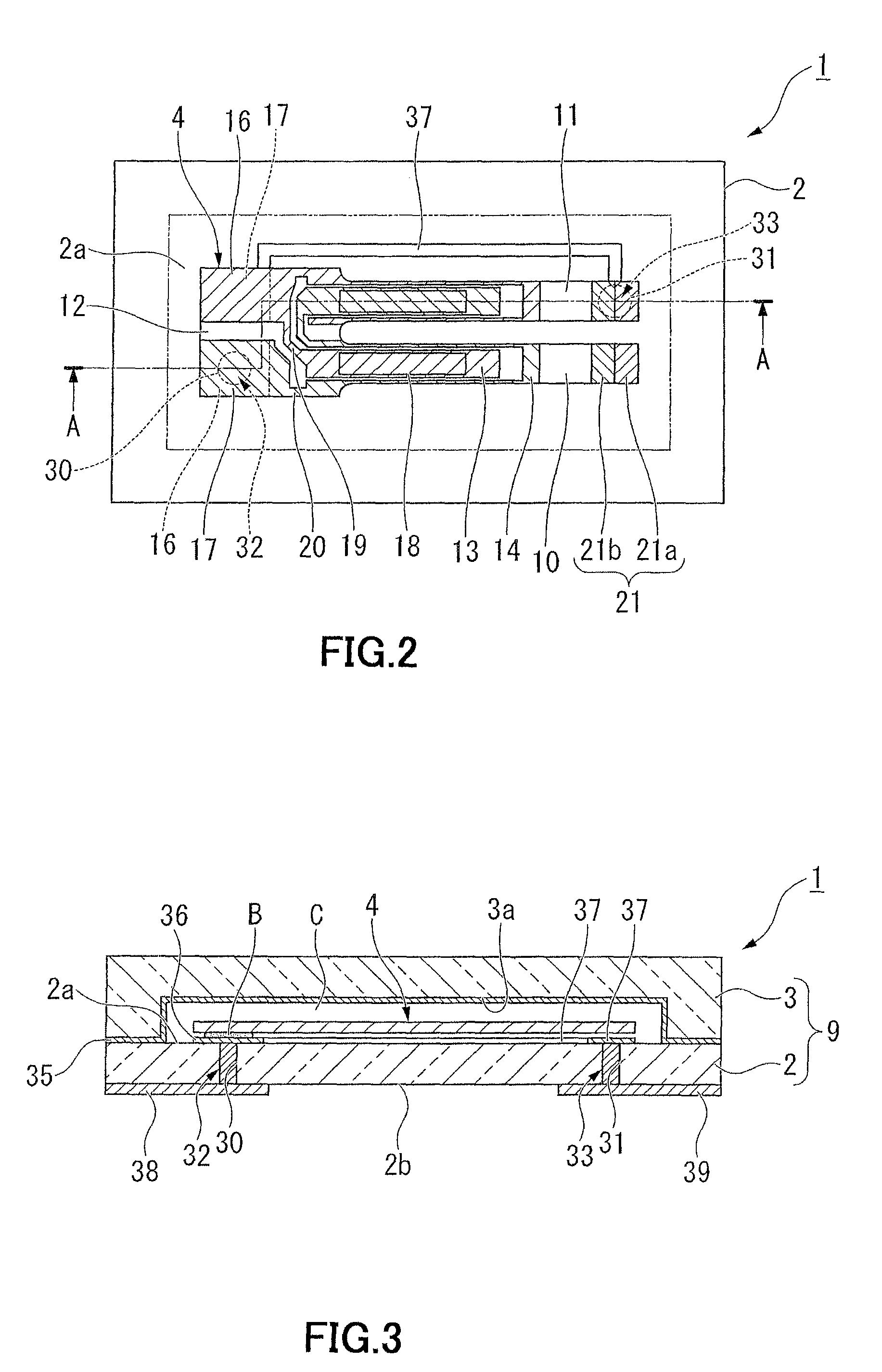
[0046]Hereinafter, a piezoelectric vibrator according to an embodiment of the present invention will be described with reference to the drawings. FIG. 1 is a perspective view showing an external appearance of a piezoelectric vibrator according to an embodiment of the present invention. FIG. 2 is a top view showing a state where a lid board of the piezoelectric vibrator is removed. FIG. 3 is a side sectional view taken along the line A-A in FIG. 2. FIG. 4 is an exploded perspective view of the piezoelectric vibrator. In FIG. 4, for better understanding of the drawings, illustrations of the excitation electrode 15, extraction electrodes 19 and 20, mount electrodes 16 and 17, and weight metal film 21 of the piezoelectric vibrating reed 4, which will be described later, are omitted.

[0047]As shown in FIGS. 1 to 4, a piezoelectric vibrator 1 according to the present embodiment is an SMD-type piezoelectric vibrator 1 including: a package 9 having a base board 2 and a ...


PUM

PropertyMeasurementUnit
softening pointaaaaaaaaaa
voltageaaaaaaaaaa
resonance frequenciesaaaaaaaaaa

Abstract

Providing a method for manufacturing a package capable of achieving reliable anodic bonding between the bonding material and a base board wafer even when the bonding material having a large resistance value is used. Providing a method for manufacturing a package by anodically bonding a bonding material, which is fixed in advance to an inner surface of a lid board wafer made of an insulator, to an inner surface of a base board wafer made of an insulator, the method including an anodic bonding step where an auxiliary bonding material serving as an anode is disposed on an outer surface of the lid board wafer, a cathode is disposed on an outer surface of the base board wafer, and a voltage is applied between the auxiliary bonding material and the cathode, wherein the auxiliary bonding material is made of a material that causes an anodic bonding reaction between the auxiliary bonding material and the lid board wafer in the anodic bonding step.

Description

RELATED APPLICATIONS[0001]This application claims priority under 35 U.S.C. §119 to Japanese Patent Application No. 2009-194468 filed on Aug. 25, 2009, the entire content of which is hereby incorporated by reference.BACKGROUND OF THE INVENTION[0002]1. Field of the Invention[0003]The present invention relates to a method for manufacturing a package, a method for manufacturing a piezoelectric vibrator, and an oscillator, an electronic device, and a radio-controlled timepiece each having the piezoelectric vibrator.[0004]2. Description of the Related Art[0005]Recently, a piezoelectric vibrator utilizing quartz or the like is used in a cellular phone and a portable information terminal as the time source, the timing source of a control signal, a reference signal source, and the like. Although there are various piezoelectric vibrators of this type, an SMD-type piezoelectric vibrator is known as one example thereof. As the piezoelectric vibrator of this type, a three-layered piezoelectric v...

Claims


Application Information

Patent Timeline
Patent Type & Authority Patents(United States)
IPC IPC(8): G04R20/10H03H3/02H03H9/21H03H9/10H01L23/02H03B5/32H03H9/02
CPCH03H9/21H03H9/1021H03H2003/022G04R20/10H03H3/02Y10T29/49005Y10T29/42Y10T29/49574Y10T29/49126
Inventor SUGIYAMA, TAKESHI
Owner SEIKO INSTR INC
Why Eureka
Try Eureka