

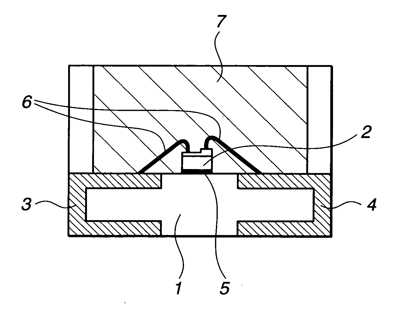
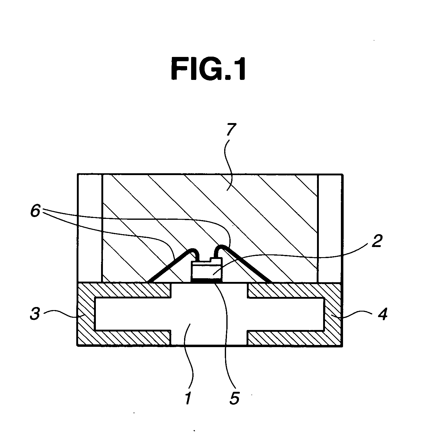
Preparation of semiconductor device
a technology of semiconductor devices and semiconductor components, applied in the direction of semiconductor/solid-state device details, dressings, coatings, etc., can solve the problems of current packages giving rise to problems, and achieve the effect of high reliability
- Summary
- Abstract
- Description
- Claims
- Application Information
AI Technical Summary
Benefits of technology
Problems solved by technology
Method used
Image

Examples
example
[0078] Preparation Examples, Examples and Comparative Examples are given below for illustrating the invention, but the invention is not limited thereto.
Preparation of Primer A
[0079] A primer composition was prepared by mixing 7 g of 3-glycidoxypropyltrimethoxysilane, 3 g of tetrabutoxytitanate, and 90 g of toluene and filtering the solution through a filter having a pore diameter of 0.8 μm.
Preparation of Primer B
[0080] A reactor was charged with 0.5 mol of 2-(3,4-epoxycyclohexylethyl)trimethoxysilane and 0.5 mol of vinyltrimethoxysilane, to which 3.0 mol of deionized water was added. Hydrolysis reaction took place at 40° C. for 8 hours. The hydrolytic condensate thus obtained was dissolved in methanol and the solution was filtered through a filter having a pore diameter of 0.8 μm. From the filtrate, the solvent was distilled off in vacuum at 80° C. and 2 mmHg. By mixing 7 g of the siloxane oligomer thus obtained, 90 g of methanol, and 3 g of zinc octylate, and filtering the so...
PUM
| Property | Measurement | Unit |
|---|---|---|
| Transparency | aaaaa | aaaaa |
Abstract
Description
Claims
Application Information