Nitride semiconductor light-emitting device and method of manufacture thereof

a technology of semiconductor light-emitting device and semiconductor light-emitting device, which is applied in the direction of semiconductor device, semiconductor laser, laser, etc., can solve the problems of insufficient formation of separation layer, insufficient adhesion, and minute cracks and exfoliation, so as to enhance the adhesion effect and increase the adhesion

Active Publication Date: 2007-04-12
SHARP FUKUYAMA LASER CO LTD
View PDF13 Cites 33 Cited by
  • Summary
  • Abstract
  • Description
  • Claims
  • Application Information

AI Technical Summary

Benefits of technology

[0016] Since the separation layer is very thin, cleaning it with an inert gas and thereby removing as much moisture and oxide film as possible at the end face of the cavity where the separation layer is going to be formed helps increase the adhesion to the end face, and thus helps enhance the effects of the adhesio...

Problems solved by technology

When a film of aluminum nitride is formed on an end face of a cavity produced by cleaving a nitride semiconductor, the film is closely packed, but contains high internal stresses, which may cause minute cracks and exfoliation.
On the other hand, when given a layer thickness less than 1 nm...

Method used


Image

  • Nitride semiconductor light-emitting device and method of manufacture thereof
  • Nitride semiconductor light-emitting device and method of manufacture thereof
  • Nitride semiconductor light-emitting device and method of manufacture thereof

Examples


first embodiment

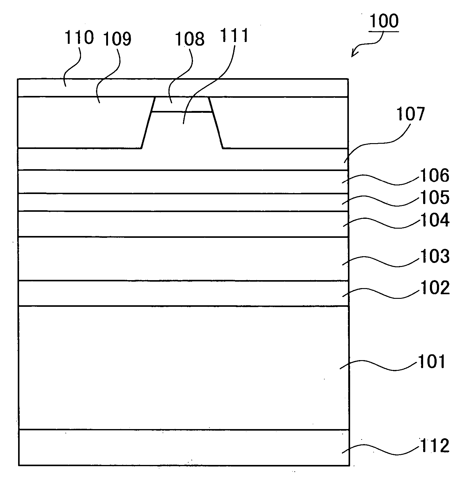
[0026] A nitride semiconductor wafer having laser structures and electrodes formed thereon is cleaved into bars by scribing and breaking processes using a diamond point. FIG. 1 is a cross-sectional view of a nitride semiconductor laser bar, taken along a direction perpendicular to the length of the cavity. The nitride semiconductor laser bar 100 has the following layers formed on an n-type GaN substrate 101, in the order named therefrom: an n-AlGaInN buffer layer 102, an n-AlGaInN clad layer 103, an n-AlGaInN guide layer 104, an AlGaInN multiple quantum well active layer 105, a p-AlGaInN guide layer 106, a p-AIGaInN clad layer 107, and a p-AlGaInN contact layer 108. These nitride semiconductor layers can be formed of group III-V nitride semiconductors.

[0027] The active layer 105 may contain about 0.01% to 10% of a group V material such as As or P. In at least part of the p-AlGaInN guide layer 106, the p-AlGaInN clad layer 107, and the p-AlGaInN contact layer 108, there is provided ...

second embodiment

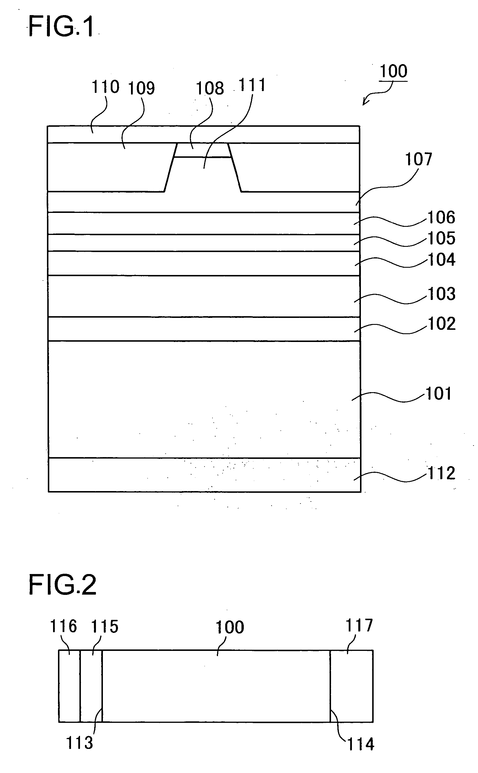
[0045] Next, a second embodiment of the present invention will be described. The second embodiment is the same as the first embodiment except that, in the second embodiment, a separation layer is formed exclusively of aluminum nitride.

[0046] The nitride semiconductor laser bar of the second embodiment has the structure shown in FIG. 2, but the separation layer 115 is formed exclusively of aluminum nitride. The nitride semiconductor layers have the same structure as in the first embodiment. The end face coating film 116 is formed of aluminum oxide, and the end face coating film 117 is formed of a multilayer film of aluminum oxide / TiO2.

[0047] A suitable material for the low-reflectivity end face coating film 116 formed on the cavity end face 113 of the nitride semiconductor laser bar 100 is aluminum oxide, because it is transparent in a short wavelength region about 400 nm, because it develops comparatively low stresses, though depending on film formation conditions, and because it ...


PUM


Abstract

In a nitride semiconductor laser bar including a group III-V nitride semiconductor layer, on the front-side cavity end face, a separation layer of aluminum nitride is laid, and further on the separation layer, an end face coating film of aluminum oxide is laid. Likewise, on the rear-side cavity end face, a separation layer of aluminum nitride is laid, and further on the separation layer, an end face coating film of an aluminum oxide/TiO2 multilayer film is laid.

Description

[0001] This nonprovisional application claims priority under 35 U.S.C. § 119(a) on Patent Application No. 2005-294361 filed in Japan on Oct. 7, 2005, the entire contents of which are hereby incorporated by reference. BACKGROUND OF THE INVENTION [0002] 1. Field of the Invention [0003] The present invention relates to a nitride semiconductor light-emitting device provided with a group III-V nitride semiconductor layer and also with an end-face coating film formed on the end faces of a cavity. [0004] 2. Description of Related Art [0005] In recent years, with the demands for increasingly high densities in the storage capacity of optical discs, there have been formulated standards for BD (Blu-ray Disc) and HD-DVD (high-definition DVD) employing blue semiconductor lasers, and there have been commercialized decoders and the like therefor. These newly developed discs offer higher densities (by being ready to be formed into two-layer discs) and allow fast writing. To benefit from these advan...

Claims


Application Information

Patent Timeline
IPC IPC(8): H01L33/00H01L21/20H01S5/028
CPCB82Y20/00H01L33/44H01S5/0021H01S5/028H01S5/0282H01S5/2231H01S5/34333
Inventor KAMIKAWA, TAKESHIKAWAGUCHI, YOSHINOBU
Owner SHARP FUKUYAMA LASER CO LTD
Why Eureka
Try Eureka