Electronic component and manufacturing method thereof

a technology of electronic components and manufacturing methods, applied in the direction of impedence networks, electrical apparatus, semiconductor devices, etc., can solve the problems of insufficient suppression of corrosion of comb electrodes, possible increase in size of saw devices, and degradation of electrical properties of saw filters, etc., to achieve excellent moisture resistance and increase in size.

Inactive Publication Date: 2007-01-11
NIHON DEMPA KOGYO CO LTD
View PDF4 Cites 41 Cited by
  • Summary
  • Abstract
  • Description
  • Claims
  • Application Information

AI Technical Summary

Benefits of technology

[0027] The present invention has been made under the above circumstances, and its object is to provide an electronic component in which a piezoelectric element is mounted on a printed circuit substrate and a vibrating part is placed in a hermetic space and which is excellent in moisture resistance and capable of ensuring the electrical connection between electrodes and the hermeticity of a sealed region and further suppressing an increase in size, and a manufacturing method thereof.

Problems solved by technology

Since the organic substance generally has higher moisture permeability than inorganic substances such as metal, there is a possibility that corrosion of the comb electrode cannot be sufficiently suppressed.
In these SAW devices, for example, it is thought to suppress the corrosion by forming a protective film made of SiO2 (silicon oxide) on the comb electrode or increasing the thickness of the exterior resin, but when the protective film is formed, this protective film influences the vibration of the comb electrode, which may cause a degradation in the electrical property of the SAW filter.
Moreover, when the thickness of the exterior resin is increased, these SAW devices may possibly increase in size.
As a result, a reduction in the size of the SAW device may possibly be hindered.
Further, in the SAW device described in Patent Document 4, the first metal layer is provided on the entire peripheral side face of the piezoelectric substrate of the SAW filter, but considering that the SAW filter is generally manufactured by being cut to have a predetermined size after comb electrodes are formed on the piezoelectric substrate and that the thickness of one piezoelectric substrate is, for example, from about 0.3 mm to about 0.5 mm, it is technically difficult to provide the metal layer on the entire peripheral side face of the piezoelectric substrate as described above, and even if it can be realized, it may cost a lot.
This may cause an increase in the size of the SAW device.
Moreover, in the SAW device described in Patent Document 5, the thermocompression bonding between the first metal layer and the second metal layer is performed simultaneously with the termocompression bonding between the input / output electrodes and the substrate electrodes, but the printed circuit substrate is usually composed of ceramics or the like and therefore sometimes warps, which makes it difficult to uniformly thermocompression-bonding the electrodes and the metal layers, and raises a concern about problems such as poor connection and non-ensuring of hermeticity.

Method used


Image

  • Electronic component and manufacturing method thereof
  • Electronic component and manufacturing method thereof
  • Electronic component and manufacturing method thereof

Examples


Embodiment Construction

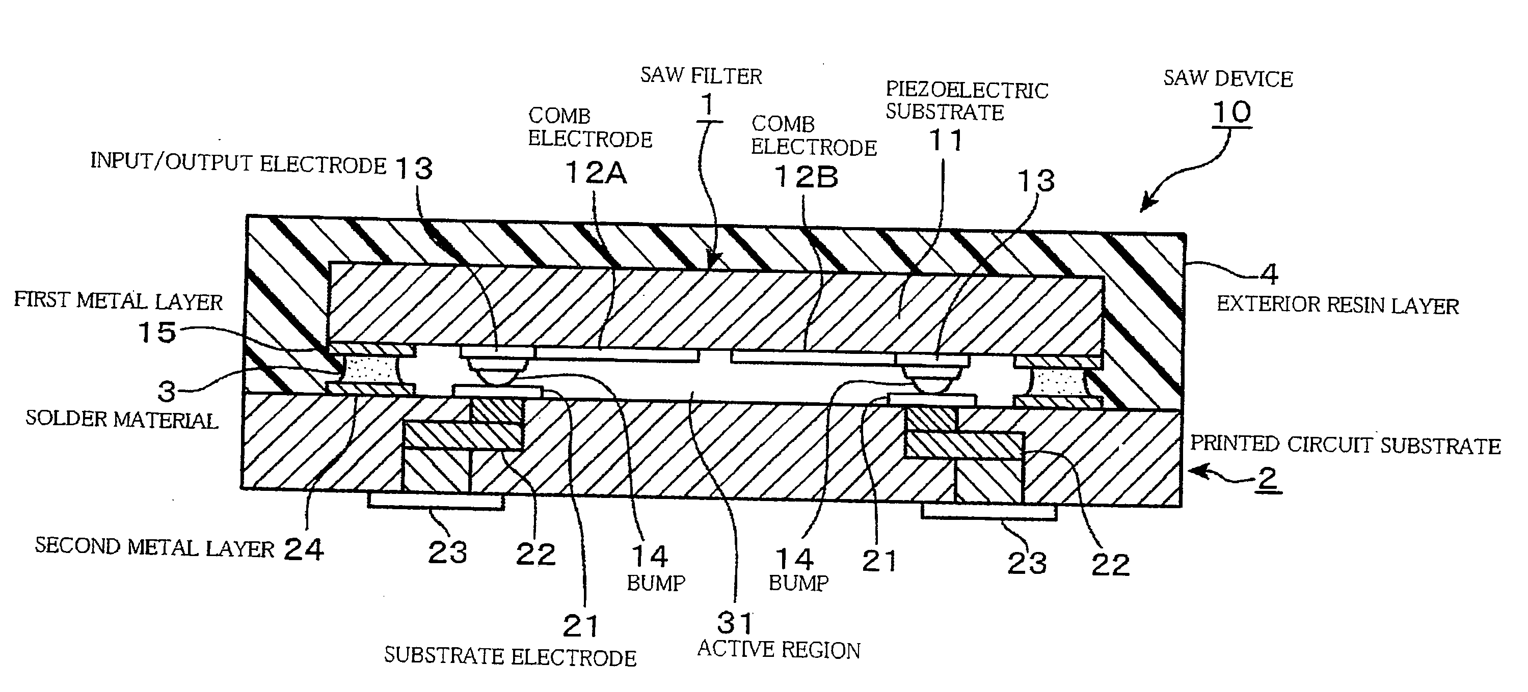
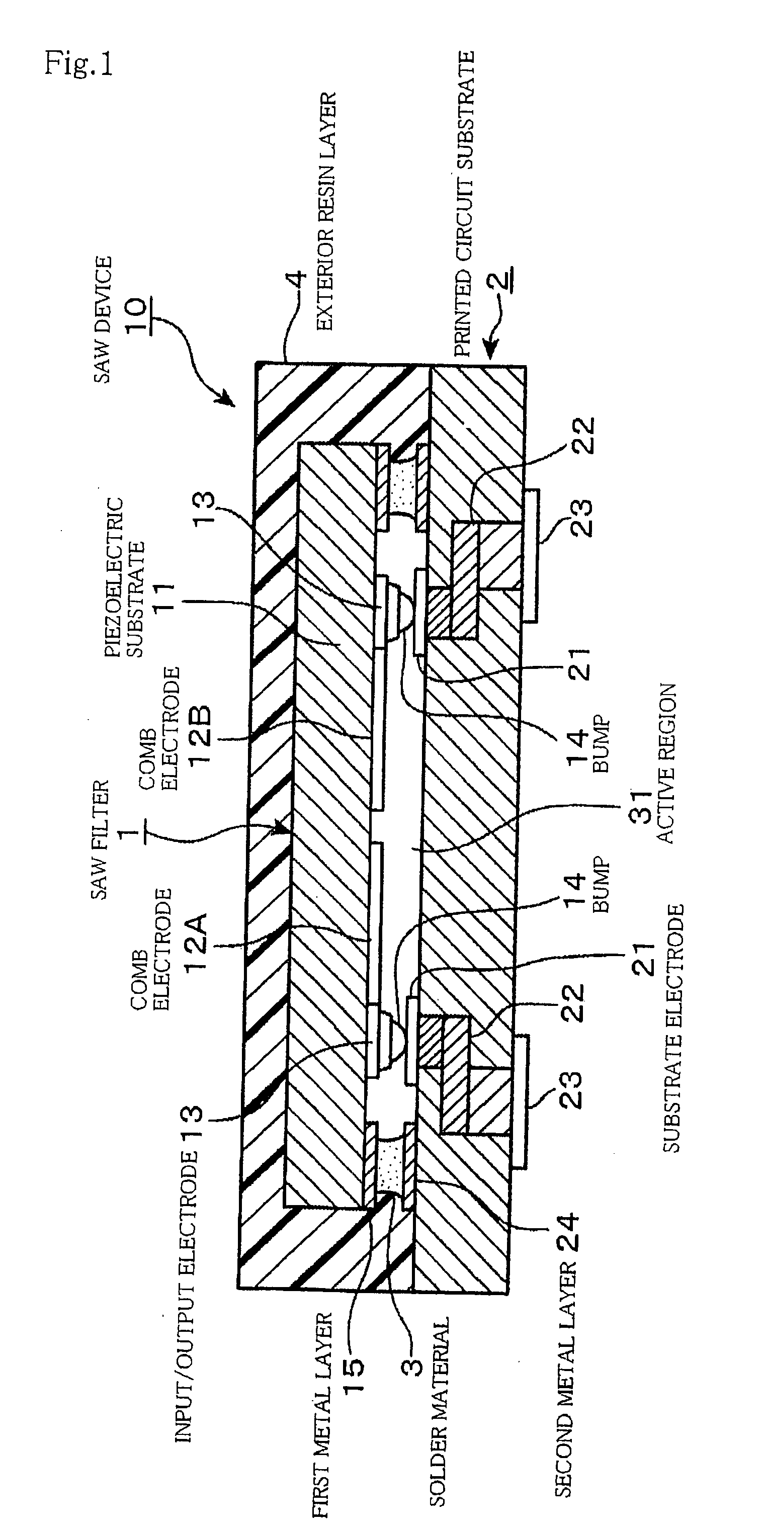
[0042] An embodiment in which an electronic component according to the present invention is applied to a SAW device 10 including a SAW filter being one of SAW elements as a piezoelectric element will be described with reference to the drawings. As shown in FIG. 1, this SAW device 10 is constituted by a SAW filter 1 being the SAW element, a printed circuit substrate 2, a solder material 3 being a sealing member, and an exterior resin layer 4. Note that in this specification, an electronic component including he SAW element is called the SAW device.

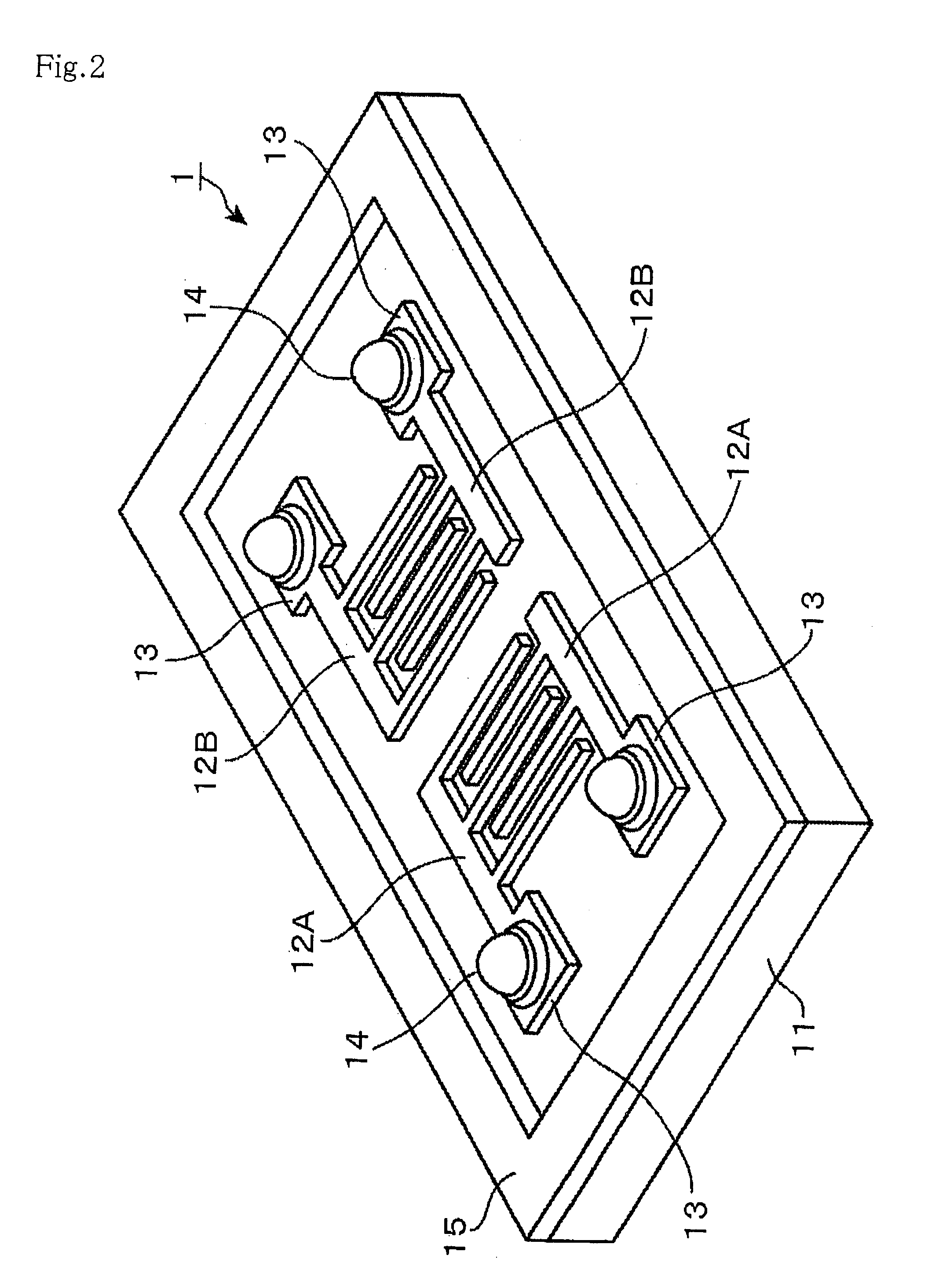
[0043]FIG. 2 is a perspective view of the SAW filter 1 seen from the side of a functional face (surface) side, numeral 11 denotes a piezoelectric substrate, and numerals 12A and 12B each denote a pair of comb electrodes (IDT) constituting a vibrating part. Numeral 13 denotes an input / output electrode being a first electrode, for example, made of Au (gold) and provided an end portion on the external side of each of the comb electrodes 12A a...


PUM


Abstract

There is provided an electronic component excellent in moisture resistance capable of ensuring electrical connection between electrodes and hermeticity of a sealed region including a vibrating part and suppressing an increase in size. An electronic component including a piezoelectric element provided with a vibrating part and a first electrode on one face of a piezoelectric substrate and a printed circuit substrate having a second electrode is constituted by including: a bump provided in advance on one of the first electrode and the second electrode and connected to the other of the first electrode and the second electrode; an annular first metal layer surrounding the vibrating part; and a solder material with a solidus temperature lower than the bump, sealing a space between the first metal layer and the printed circuit substrate to make a placement region of the vibrating part a hermetic space, whereby moisture permeation into the hermetic space and the outward spread of the solder material can be suppressed, and a space for the bump to spread by being melted can be omitted. Moreover, the electrical connection between the electrodes and the sealing of the placement region can be performed in separate processes, so that high hermeticity can be obtained.

Description

BACKGROUND OF THE INVENTION [0001] 1. Field of the Invention [0002] The present invention relates to an electronic component including a piezoelectric element provided with vibrating part which generates a vibrational wave on a substrate and a manufacturing method thereof. [0003] 2. Description of the Related Art [0004] As an example of a piezoelectric element, there is a surface acoustic wave (SAW) element. This SAW element is an element which uses a surface acoustic wave propagating along the surface of a solid body and, for example, has a structure in which plural comb electrodes making pairs called ITDs are provided on one face of a piezoelectric substrate. When an electrical signal is applied to comb electrodes making one pair, an electric field is generated around these comb electrodes, a SAW generated by excitation of these comb electrodes propagates along the surface of the piezoelectric substrate to excite comb electrodes making another pair, and the SAW is converted into a...

Claims


Application Information

Patent Timeline
Patent Type & Authority Applications(United States)
IPC IPC(8): H03H9/64
CPCH03H3/08H03H9/1085H03H9/059H03H9/02937H01L2224/16225H01L2224/05024H01L2224/05008H01L2224/05001H01L2224/05144H01L2224/05644H01L2924/00014H01L2224/02379H01L2224/0615H01L24/05H01L2224/05099
Inventor TSUDA, TOSHIMASAABE, SEIJISAKAI, MINORUSAKAIRI, NATSUHIKO
Owner NIHON DEMPA KOGYO CO LTD
Why Eureka
Try Eureka