Combined APD / PIN InGaAs photodetector with microlens structure and method of manufacture
- Summary
- Abstract
- Description
- Claims
- Application Information
AI Technical Summary
Benefits of technology
Problems solved by technology
Method used
Image

Examples
Embodiment Construction
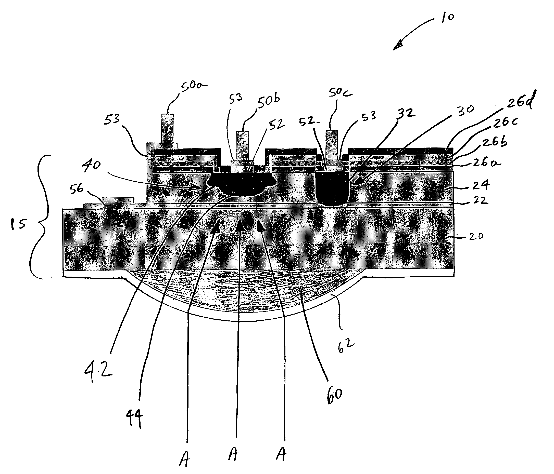
[0016] The present invention relates to an InGaAs photodetector having an avalanche photodiode (APD) and a p-intrinsic-n (PIN) photodiode, wherein high (e.g., 100%) optical fill factors are provided for both the APD and the PIN photodiode. The photodetector can be used for both ranging and imaging applications, can be formed as a single pixel, and multiple pixels can be fabricated to form a focal plane array. The present invention also provides a method of manufacturing such a photodiode.
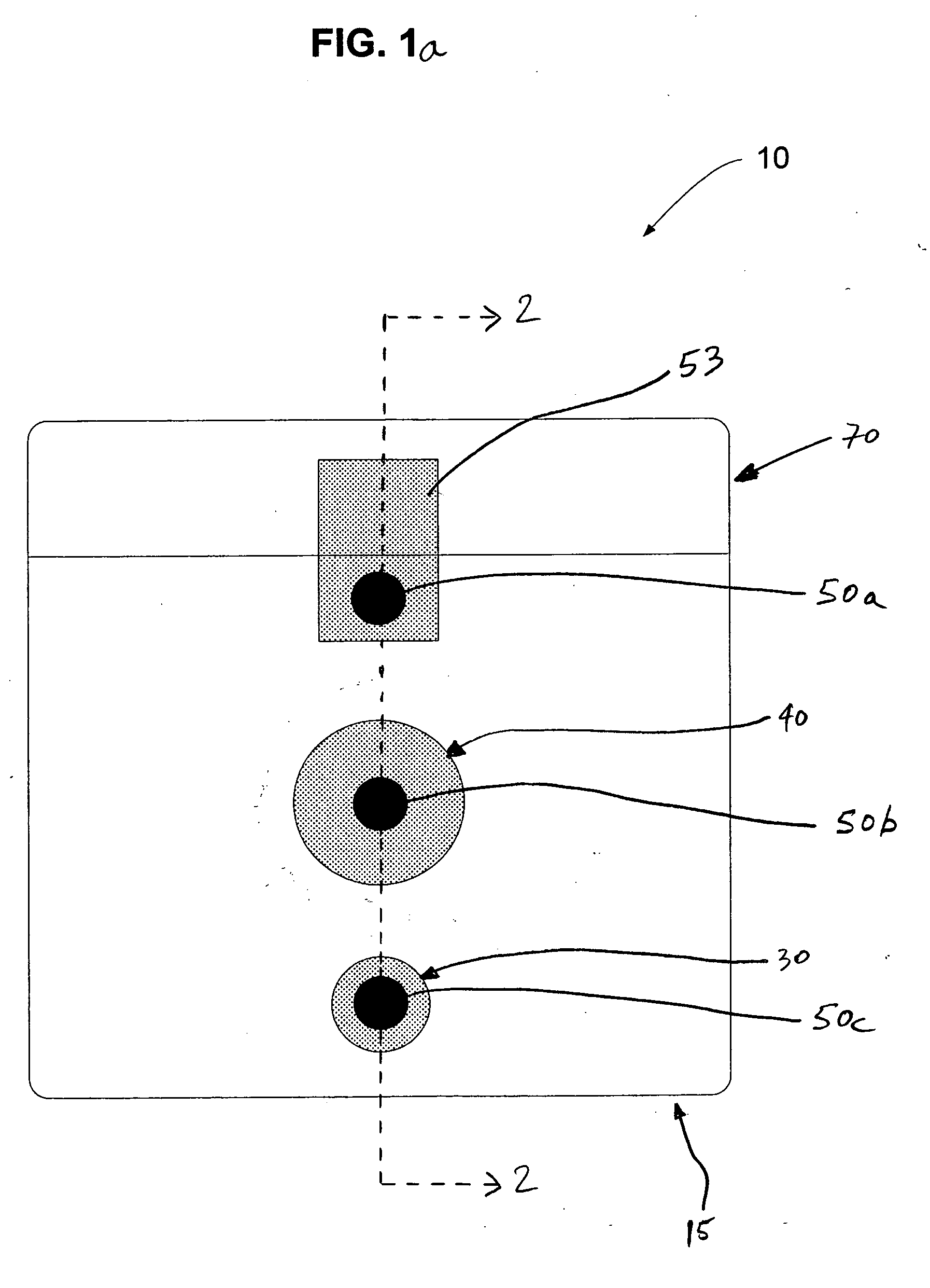
[0017]FIG. 1a is a view of an InGaAs photodetector according to the present invention, indicated generally at 10. The photodetector 10 includes an InGaAs wafer 15, in which is formed a p-intrinsic-n (PIN) type photodiode 30 and an avalance photodiode (APD) 40. The APD 40 is formed in a central region of the photodetector 10. The PIN photodiode 30 could be formed in any desired geometry and positioned at any desired location in the InGaAs wafer 15 outside of the central region occupied by the APD 40...
PUM
 Abstract
Description
Claims
Application Information
 - R&D
- Intellectual Property
- Life Sciences
- Materials
- Tech Scout
- Unparalleled Data Quality
- Higher Quality Content
- 60% Fewer Hallucinations
Browse by: Latest US Patents, China's latest patents, Technical Efficacy Thesaurus, Application Domain, Technology Topic, Popular Technical Reports.
© 2025 PatSnap. All rights reserved.Legal|Privacy policy|Modern Slavery Act Transparency Statement|Sitemap|About US| Contact US: help@patsnap.com