Supercharge Your Innovation With Domain-Expert AI Agents!

Organic semiconductor mixed material and organic photovolatic device using the same

a technology of organic photovoltaic devices and mixed materials, which is applied in the direction of semiconductor devices, photovoltaic energy generation, electrical apparatus, etc., can solve the problems of limiting the performance development difficult organic photoelectric devices made of binary blended materials, and climate change. achieve the effect of improving the power conversion efficiency and fill factor of organic photoelectric devices

Pending Publication Date: 2021-02-11
RAYNERGY TEK INC
View PDF2 Cites 2 Cited by
  • Summary
  • Abstract
  • Description
  • Claims
  • Application Information

AI Technical Summary

Benefits of technology

The organic semiconductor mixed material in this patent can improve the performance of organic photoelectric devices by increasing power conversion efficiency and fill factor.

Problems solved by technology

In view of global warming, climate change has become a common challenge in the international communities.
However, because the organic photoelectric devices are limited by the “narrow absorption” characteristics of the organic materials, it is difficult for the organic photoelectric devices made of the binary blended materials to effectively utilize the broad spectrum of the solar energy, and there is always contradictory between phase blending (favorable to exciton dissociation) and phase separation (favorable for charge transport), which in turn restricts the performance development of the organic photoelectric devices.
However, the current ternary organic photoelectric devices are faced with the problems of difficulty in controlling morphology and maintaining high-efficient excitons dissociation and charge transport at same time.
As a result, the power conversion efficiency (PCE) and fill factor (FF) of the organic photoelectric devices are difficult to be effectively improved at the same time.
Therefore, how to provide an organic semiconductor mixed material with controllable active layer morphology, high power conversion efficiency and high fill factor, and an organic photoelectric device using the same are an important issue at present.

Method used


Image

  • Organic semiconductor mixed material and organic photovolatic device using the same
  • Organic semiconductor mixed material and organic photovolatic device using the same
  • Organic semiconductor mixed material and organic photovolatic device using the same

Examples


Embodiment Construction

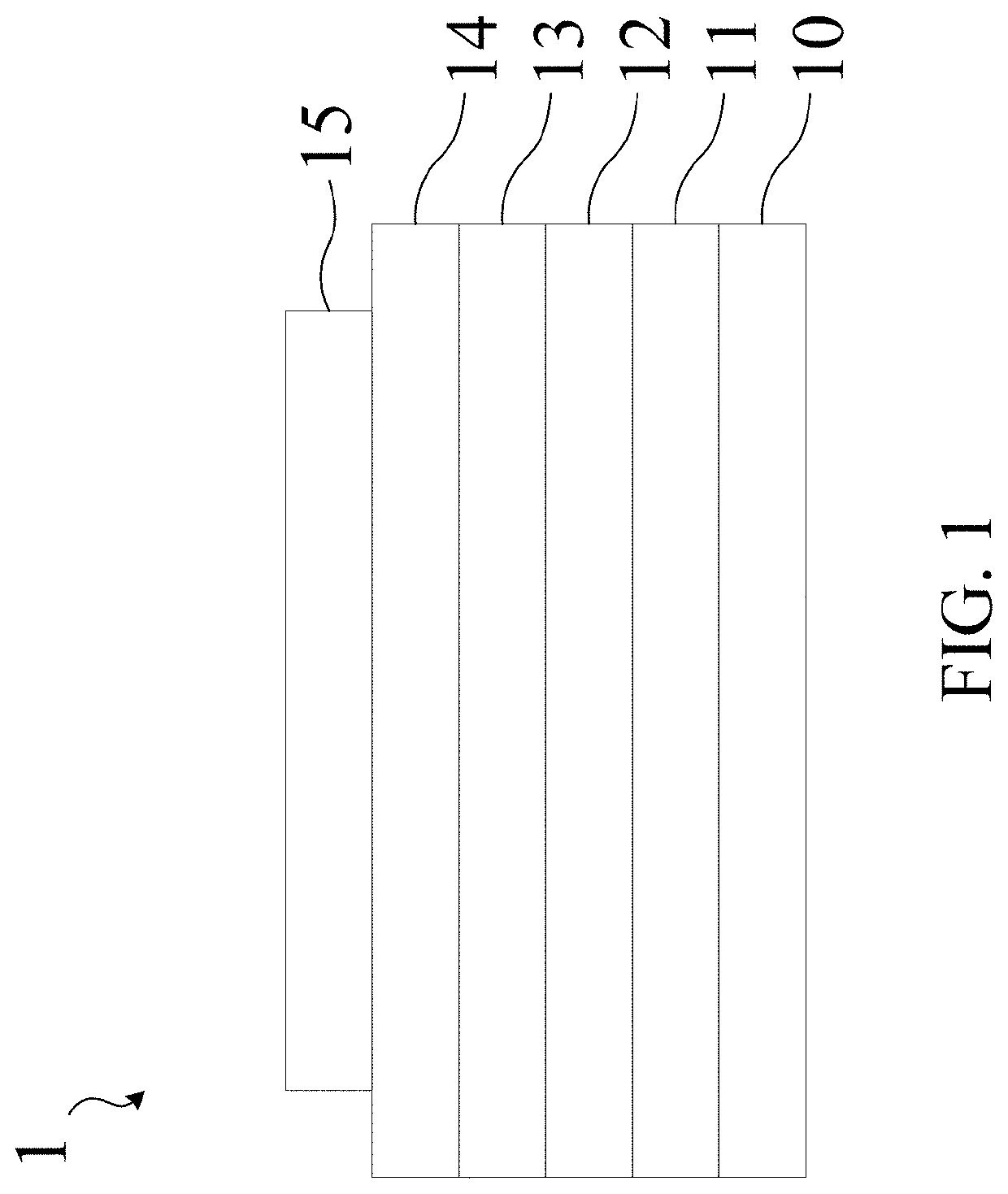
[0031]In order to make the advantages, spirit and features of the present invention easier and clearer, it will be detailed and discussed in the following with reference to the embodiments and the accompanying drawings. It is worth noting that the specific embodiments are merely representatives of the embodiments of the present invention, but it can be implemented in many different forms and is not limited to the embodiments described in this specification. Rather, these embodiments are provided so that this disclosure will be thorough and complete.

[0032]The terminology used in the various embodiments disclosed in the present invention is only for the purpose of describing specific embodiments, and is not intended to limit the various embodiments disclosed in the present invention. As used herein, singular forms also include plural forms unless the context clearly indicates otherwise. Unless otherwise defined, all terms (including technical and scientific terms) used in this specifi...


PUM

PropertyMeasurementUnit
Fractionaaaaaaaaaa
Fractionaaaaaaaaaa
Fractionaaaaaaaaaa

Abstract

Organic photovoltaic device comprises a first electrode, a first carrier transfer later, an active layer, a second carrier transfer layer and a second electrode. The first electrode is a transparent electrode. The active layer includes at least one electron donor, a first electron acceptor, and a second electron acceptor. Wherein, the electron donor is an organic polymer. The first electron acceptor is a crystalline material, and the self-molecule stacking distance of the first electron acceptor is less than 4 Å. The second electron acceptor is a crystal destruction material, and the second electron acceptor includes a fullerene derivative. The organic photovoltaic device of the present invention not only has a controllable morphology formation but also can enhance fill factor and improve power conversion efficiency.

Description

[0001]The present application is based on, and claims priority from, U.S. provisional patent application No. 62 / 884,348, filed on Aug. 8, 2019, the disclosure of which is hereby incorporated by reference herein in its entirety.BACKGROUND OF THE INVENTIONField of the Invention[0002]The present invention relates to an organic semiconductor mixed material applied to an organic photoelectric device, and an organic photoelectric device including the said organic semiconductor mixed material.Description of the Prior Art[0003]In view of global warming, climate change has become a common challenge in the international communities. The Kyoto protocol proposed by the “United Nations Framework Convention on Climate Change (UNFCCC)” in 1997 which had entered into force in 2005 is aimed at reducing carbon dioxide emissions. In this regard, countries are focusing on the development of renewable energy to reduce the use of petrochemical fuels. As the sun provides far enough energy needs of people ...

Claims


Application Information

Patent Timeline
IPC IPC(8): H01L51/00H01L51/42
CPCH01L51/0074H01L51/0058H01L51/0053H01L51/4253H01L51/0094H01L51/0047H01L51/0071H10K85/215H10K85/655H10K85/6576H10K85/6572H10K85/657H10K85/40H10K50/11H10K30/30H10K30/50Y02E10/549H10K85/113H10K85/151H10K85/621H10K85/626
Inventor CHANG, YI-MINGLI, CHIA-HUATAN, HUEI-SHUAN
Owner RAYNERGY TEK INC
Features
  • R&D
  • Intellectual Property
  • Life Sciences
  • Materials
  • Tech Scout
  • Unparalleled Data Quality
  • Higher Quality Content
  • 60% Fewer Hallucinations
Learn More