Compact active pixel with low-noise snapshot image formation

a snapshot image and active pixel technology, applied in the field of electronic imaging devices, can solve the problems of low noise, inability to normally provide the reset signal of each pixel, and uncertainty about the voltage of each photo-detector, so as to efficiently reset the pixel, reduce the noise, and reduce the noise

Inactive Publication Date: 2005-11-15
SAMSUNG ELECTRONICS CO LTD
View PDF37 Cites 16 Cited by
  • Summary
  • Abstract
  • Description
  • Claims
  • Application Information

AI Technical Summary

Benefits of technology

[0008]In general, the present invention comprises a low-noise imaging system for implementation in CMOS or in other semiconductor fabrication technologies. The low-noise amplifier system efficiently suppresses reset (kTC) noise by using a compact preamplifier consisting of a photodetector and only four MOSFETs of identical polarity in conjunction with ancillary circuits located on the CMOS imager's periphery. The supporting circuits help the simplified pixel circuit to synchronously acquire (i.e., take a snapshot) an image across an imaging array, read the signal with low noise, and efficiently reset the pixel with low noise.
[0009]The low noise amplifier system of the present invention is formed by the aggregate circuitry in each pixel, the supporting circuitry in the column buffer amplifier and the row-based circuitry, and the waveform generation circuits servicing each column and row of pixels. The signals from the active pixels are read out by the low-noise signal amplification system consisting of the pixel comprised of only four MOSFETs, the waveform generators and a standard column buffer. In addition to circuitry for suppressing the detector's reset noise, the column buffer in the downstream electronics typically performs additional signal processing, sample-and-hold, optional video pipelining, and column amplifier offset cancellation functions to suppress the temporal and spatial noise that would otherwise be generated by the column buffer.
[0010]The low-noise system of the present invention provides the following key functions: (1) provides true “snapshot” image formation; (2) suppresses reset noise without having to provide analog memory to facilitate correlated double sampling; (3) provides high sensitivity via source follower amplification with small sense capacitance; (4) minimizes demand on amplifier bandwidth to avoid generation of fixed pattern noise due to variations in amplifier time constant and stray capacitance; (5) provides adequate power supply rejection to enable development of imaging systems-on-a-chip that do not require elaborate support electronics; and (6) is compatible with application to imaging arrays having pixel pitch well below 10 microns.
[0011]The present invention has the advantage of full process compatibility with standard silicided submicron CMOS. The present invention also helps to maximize yield and minimize die cost because the circuit complexity is distributed among the active-pixels and peripheral circuits. The spectral response is broad from the near-ultraviolet (400 nm) to the near-IR (>800 nm).
[0012]Because the present invention has only four MOSFETs in each pixel, the invention provides as-drawn optical fill factor >40% at 5 μm pixel pitch using 0.25 μm design rules in CMOS. The actual optical fill factor is somewhat larger due to lateral collection and the large diffusion length of commercial CMOS processes. Another advantage is the flexibility to collocate digital logic and signal-processing circuits due its high immunity to electromagnetic interference.
[0013]When fully implemented in the desired camera-on-a-chip architecture, the low-noise active pixel sensor (APS) can provide temporal read noise below 10 e- (at data rates compatible with either video imaging or still photography via electronic means), fixed pattern noise significantly below 0.02% of the maximum signal (on a par with competing CCD imagers), <0.5% nonlinearity, ≧1 V signal swing for 3.3 V power supply, large charge-handling capacity, and variable sensitivity using simple serial interface updated on a frame-by-frame basis via digital interface to a host microprocessor.

Problems solved by technology

A CMOS image sensor's performance, however, is often limited by the noise generated by resetting each of its photodiodes to a known potential after each electronic image, or picture, is read out.
Similarly, the reset noise (kTC) in a CMOS sensor causes uncertainty about the voltage on each photo-detector following the reset, but each pixel's reset signal is not normally available.
No CMOS foundry processes support integration of ITO electrodes due to possible wafer contamination and concomitant yield loss.
Another key issue related to incompatibility with standard CMOS technology is the difficulty in optically isolating this storage site to eliminate image smear.

Method used


Image

  • Compact active pixel with low-noise snapshot image formation
  • Compact active pixel with low-noise snapshot image formation
  • Compact active pixel with low-noise snapshot image formation

Examples


Embodiment Construction

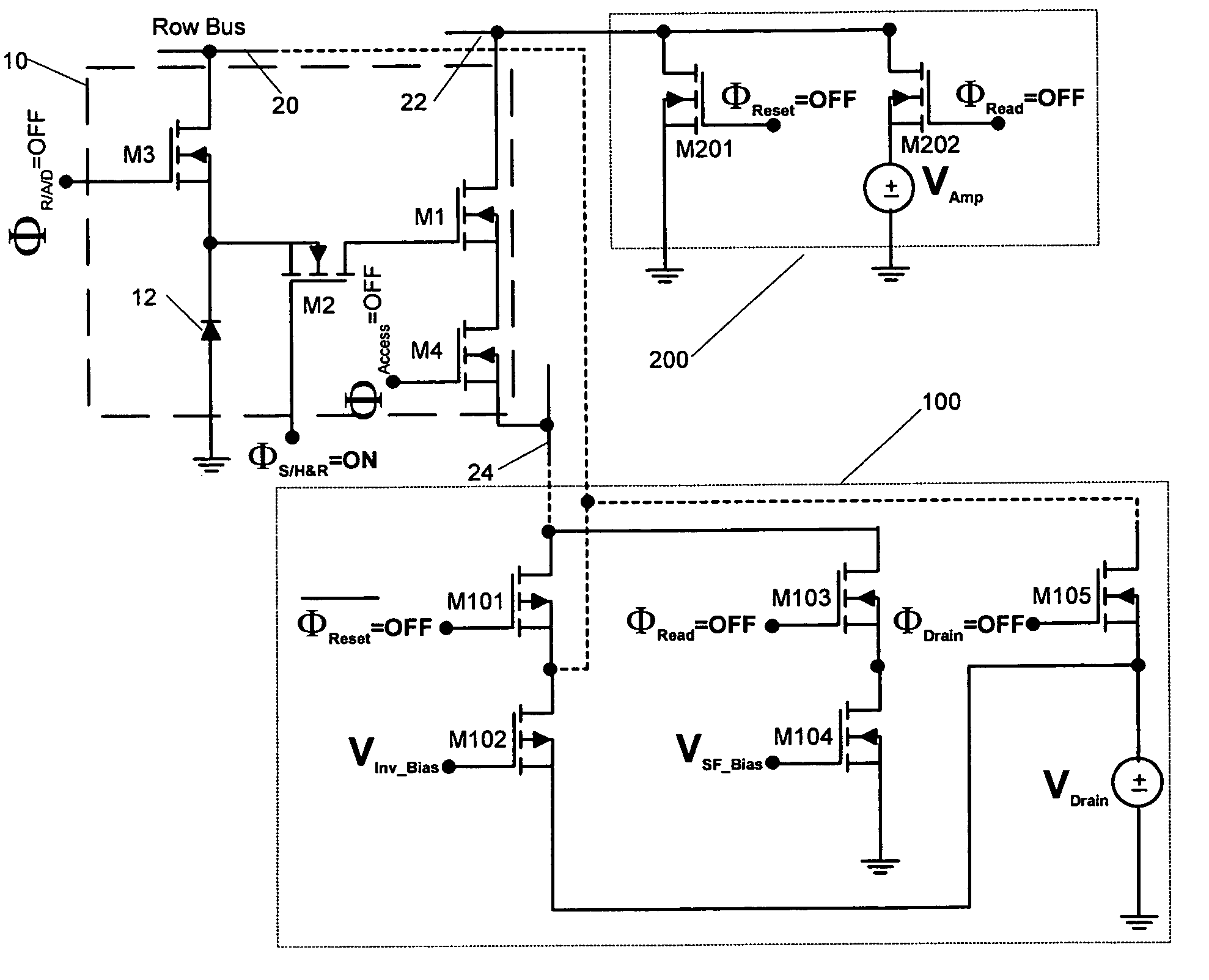
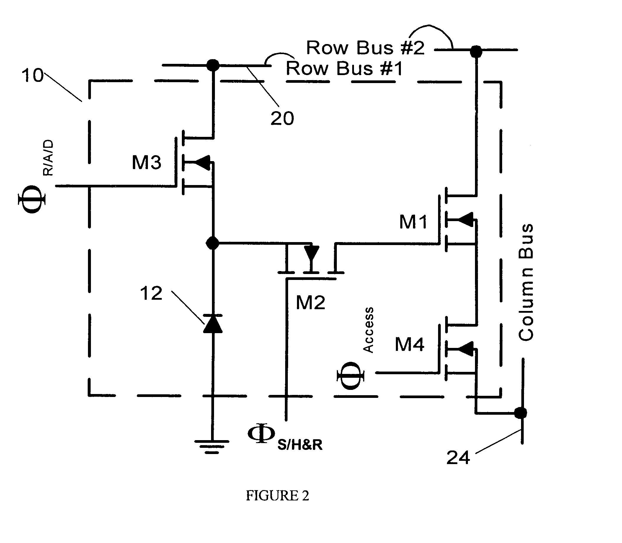
[0023]The following description is provided to enable any person skilled in the art to make and use the invention and sets forth the best modes contemplated by the inventor for carrying out the invention. Various modifications, however, will remain readily apparent to those skilled in the art, since the basic principles of the present invention have been defined herein specifically to provide a low noise CMOS image sensor circuit having “snapshot” image formation capability. Any and all such modifications, equivalents and alternatives are intended to fall within the spirit and scope of the present invention.

[0024]The CMOS readout and amplification system of the present invention includes an exemplary design for an active-pixel CMOS imager. A prototype embodiment of the low-noise APS invention can be configured, for example, as a visible imager comprising an array of 1024 (columns) by 728 (rows) of visible light detectors (photodetectors). The rows and columns of active-pixels can be...


PUM


Abstract

A low-noise active pixel circuit is disclosed that efficiently suppresses reset (kTC) noise by using a compact preamplifier consisting of a photodetector and only four MOSFETs of identical polarity, in conjunction with ancillary circuits located on an imager's periphery. The supporting circuits help the simplified pixel circuit to synchronously acquire (i.e., take a snapshot) an image across an imaging array, read the signal with low noise, and efficiently reset the pixel with low noise.

Description

BACKGROUND OF THE INVENTION[0001]1. Field of the Invention[0002]The present invention relates generally to electronic imaging devices and, more particularly, to low noise CMOS image sensors having “snapshot” image formation capability.[0003]2. Description of the Related Art[0004]Significant advances in photosensor image processing for camera and video systems are now possible through the emergence of CMOS pixel sensors. CMOS-based imaging sensors have distinct manufacturing cost savings and low power use advantages over other technologies such as charge coupled devices (CCD). A CMOS image sensor's performance, however, is often limited by the noise generated by resetting each of its photodiodes to a known potential after each electronic image, or picture, is read out. Such noise is readily suppressed in CCD-based cameras because CCD reset noise is generated on only one capacitance, i.e., the sense diffusion diode that converts the photo-generated charge to a voltage. Also, full-fram...

Claims


Application Information

Patent Timeline
Patent Type & Authority Patents(United States)
IPC IPC(8): H04N3/15H04N5/363H01L27/146
CPCH04N5/363H04N25/575H04N25/65
Inventor KOZLOWSKI, LESTER J.
Owner SAMSUNG ELECTRONICS CO LTD
Why Eureka
Try Eureka