Self-cleaning protective coatings for use with photovoltaic cells

a photovoltaic cell and self-cleaning technology, applied in the direction of metal/metal-oxide/metal-hydroxide catalysts, light radiation electric generators, physical/chemical process catalysts, etc., can solve the problems of reducing the efficiency of large planar photovoltaic cells, difficult to make semiconductor films, and crystalline silicon-based cells, so as to maintain the efficiency of photovoltaic cells, reduce cleaning and repainting efforts, and reduce the effect of labor

Inactive Publication Date: 2007-01-25
BARNES CHRISTOPHER
View PDF78 Cites 129 Cited by
  • Summary
  • Abstract
  • Description
  • Claims
  • Application Information

AI Technical Summary

Benefits of technology

[0022] To address the problems found in the prior art, the present invention provides systems and methods for maintaining the efficiency of photovoltaic cells. In particular, the present invention provides systems and methods for maintaining self-cleaning albedo surfaces and self-cleaning photovoltaic cell panels. Self-cleaning albedo surfaces and photovoltaic cell panels are produced by applying one or more layers of self-cleaning material onto the surface of photovoltaic cell panels as well as albedo surfaces. In this way, the drawbacks found in the prior art, namely laborious time consuming cleaning and repainting efforts, are minimized, thereby yielding a more efficient cost effective photovoltaic cell system.

Problems solved by technology

However, because of the expense in making crystalline silicon-based cells, thin film photovoltaic cells made of materials other than silicon have been explored and used.
However, even when a TCO layer is present, a bus bar network 114 is typically needed to draw off current since the TCO has too much resistance to efficiently perform this function in larger photovoltaic cells.
Although such cells are highly efficient when they are smaller, larger planar photovoltaic cells have reduced efficiency because it is harder to make the semiconductor films that form the junction in such photovoltaic cells uniform.
Furthermore, the occurrence of pinholes and similar flaws increase in larger planar photovoltaic cells.
These features can cause shunts across the junction.
For example, an extremely cloudy day reduces the amount of photovoltaic radiation available for absorption by a photovoltaic cell system.
High albedo materials, however, are often difficult to maintain.
Unfortunately, the albedo properties of material degrade over time.
For example, numerous factors, such as bacteria growth, dirt built up, and / or watermarks on the surface of the material can all deleteriously affect the albedo property of such material.
Such degradation in the albedo affect of materials adversely affects the efficiency of photovoltaic cell assemblies that make use of the albedo effect to improve efficiency since the efficiency of such systems is a function, in part, of the strength of such albedo effects.
However, such regular cleaning of such materials, in order to maintain their albedo properties, is inconvenient, time consuming, and expensive.
Because of this compact arrangement, the albedo surfaces around such photovoltaic cells are difficult to access for cleaning purposes.
Furthermore, use of detergents to facilitate cleaning can have adverse effects on albedo surfaces that are sensitive to such chemicals.
Clearly, such efforts are costly and time consuming.
However, such approaches are inconvenient for many of the same reasons described above in relation to cleaning regimens.
Such reasons include the difficulty in gaining access to such regions and the manual labor involved in painting.
Further, this approach is not advantageous because it typically requires a cleaning prep stage, because of the expense of the paint used, and because, over time, an excessive buildup comprising multiple layers of paint form on the albedo surface that need to be stripped away in order to maintain the integrity of such surfaces.
However, such cleaning has the same drawbacks as the cleaning of albedo surfaces.
Namely, such cleaning is time consuming, can degrade the material properties of the panels through adverse interaction (chemical, abrasive, or otherwise) with the cleaning agents, and is expensive.
However, such cleaning may be necessary since any debris build up on photovoltaic cell panel surfaces adversely affects their efficiency.

Method used


Image

  • Self-cleaning protective coatings for use with photovoltaic cells
  • Self-cleaning protective coatings for use with photovoltaic cells
  • Self-cleaning protective coatings for use with photovoltaic cells

Examples


Embodiment Construction

[0039] The present invention provides systems and materials to improve photovoltaic cell performance by implementing a self-cleaning function on photovoltaic cells and / or on albedo surfaces in the vicinity of photovoltaic cell assemblies. One aspect of the invention provides materials for protecting albedo surfaces that surround photovoltaic cell assemblies, thereby maximizing energy input into the photovoltaic cell assemblies. Another aspect of the invention provides materials for self-cleaning photovoltaic cell panels, thereby maintaining their efficiency. A third aspect of the present invention provides designs for portable albedo collecting devices that are associated with photovoltaic cell assemblies to optimize energy efficiency.

5.1 General Architecture

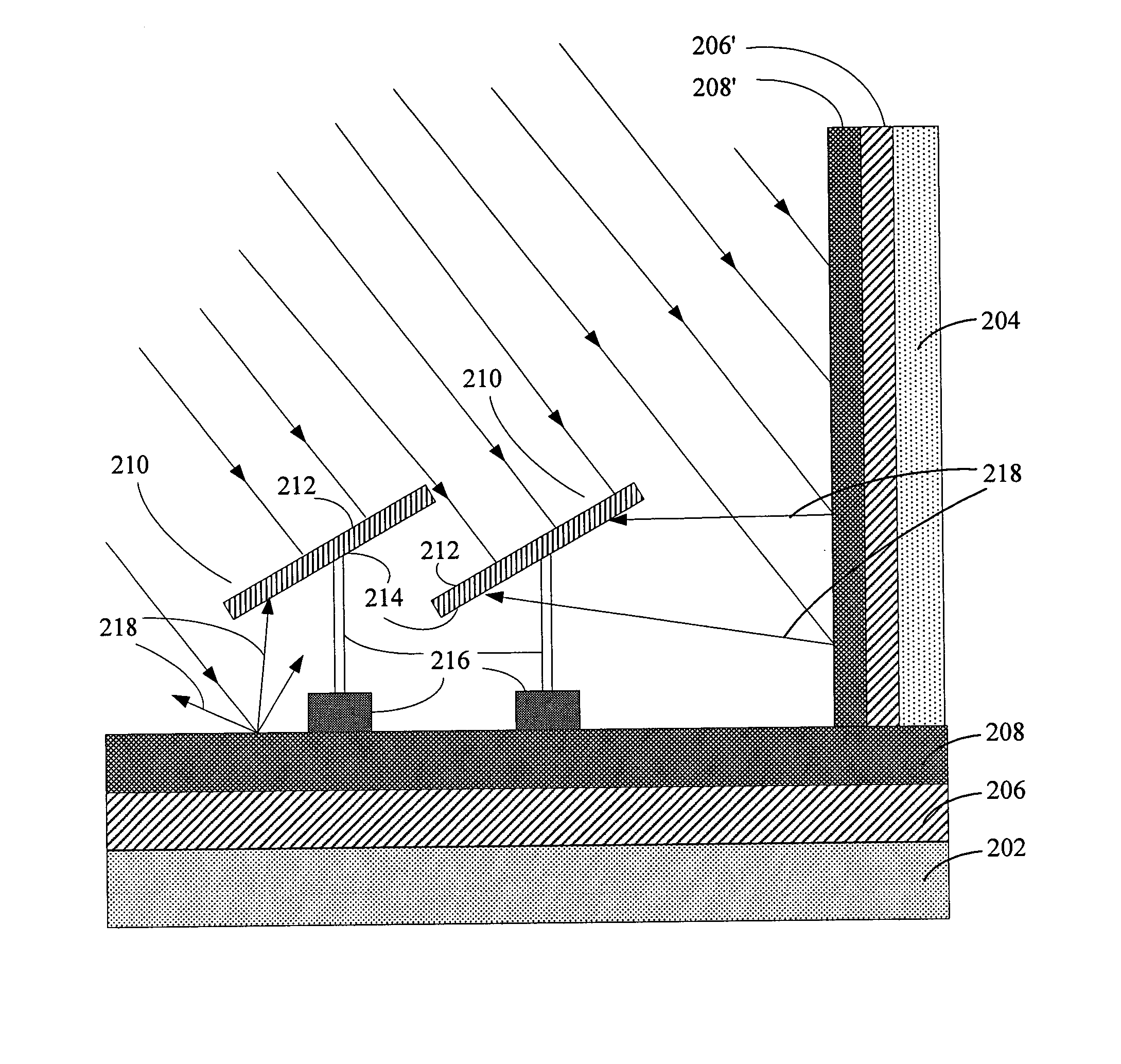
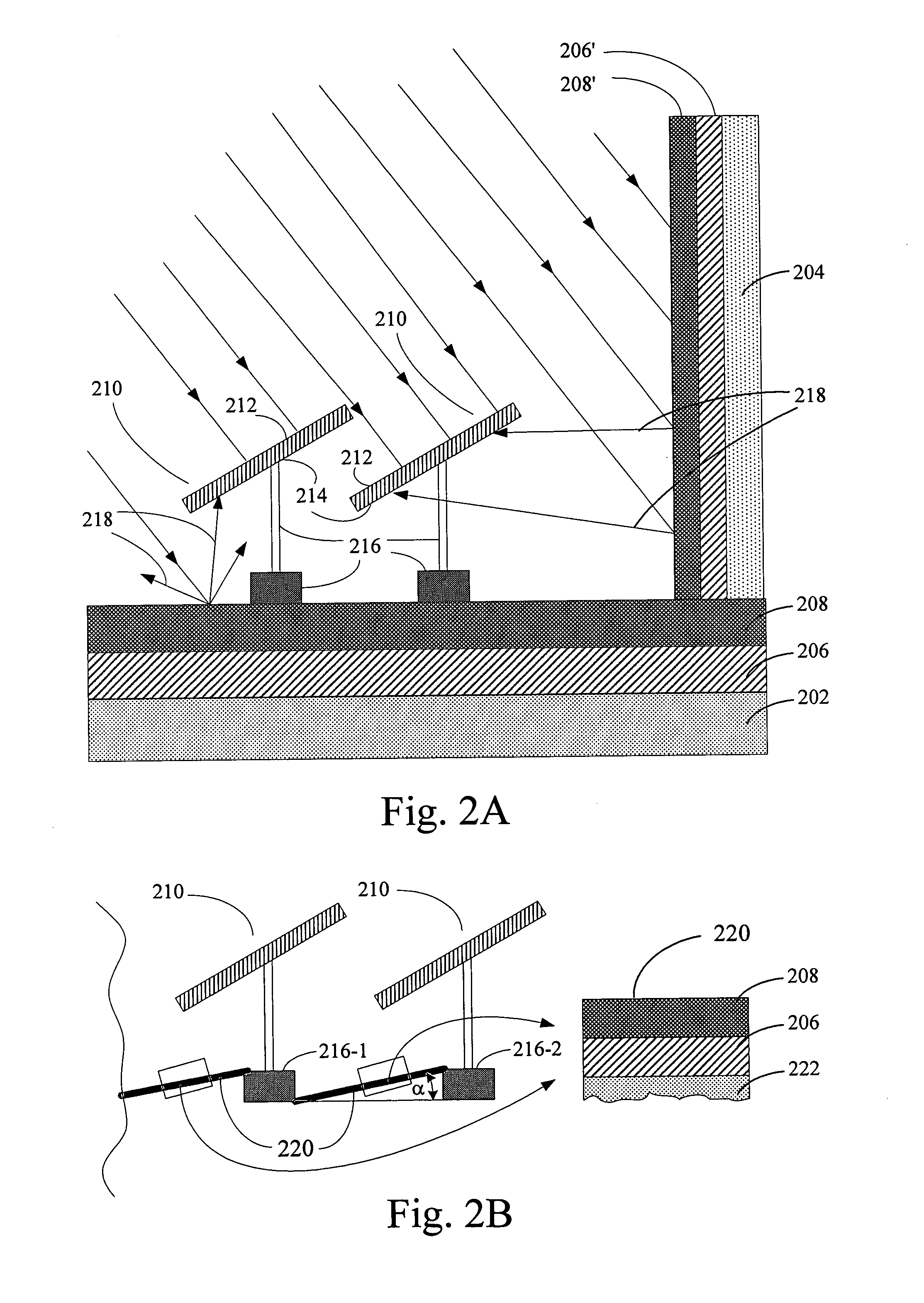
[0040] The present invention discloses systems and methods for improving existing photovoltaic cell assemblies that utilize albedo effects thereby improving their performance. As depicted in FIG. 2A, an albedo collector system...


PUM

PropertyMeasurementUnit
band gapaaaaaaaaaa
surface areasaaaaaaaaaa
thicknessaaaaaaaaaa

Abstract

Systems and materials to improve photovoltaic cell efficiency by implementing a self-cleaning function on photovoltaic cells and on albedo surfaces associated with photovoltaic cell assemblies are provided. Materials for protecting albedo surfaces that surround photovoltaic cell assemblies, thereby maximizing energy input into the photovoltaic cell assemblies, are provided. Materials for self-cleaning photovoltaic cell panels, thereby maintaining their efficiency, are provided. Portable albedo collecting devices associated with photovoltaic cell assemblies are provided.

Description

CROSS REFERENCE TO RELATED APPLICATIONS [0001] This Application claims priority to United States provisional patent Application No. 60 / 700,982, filed Jul. 19, 2005, which is hereby incorporated herein by reference in its entirety.1. FIELD OF INVENTION [0002] This invention generally relates to photovoltaic cell assemblies for converting photovoltaic energy into electrical energy and more particularly to improved photovoltaic cell energy conversion by maintaining the high albedo of surrounding environment of photovoltaic cells. 2. BACKGROUND OF THE INVENTION [0003] Interest in photovoltaic cells, also known as solar cells, has grown rapidly in the past few decades. Photovoltaic cells comprise semiconductor junctions such as p-n junctions. It is known that light with photon energy greater than the band gap of an absorbing semiconductor layer in a semiconductor junction is absorbed by the layer. Such absorption causes optical excitation and the release of free electrons and free holes ...

Claims


Application Information

Patent Timeline
Patent Type & Authority Applications(United States)
IPC IPC(8): H02N6/00
CPCH01L31/02167H01L31/02168H01L31/035281H01L31/0749H01L2924/09701Y02E10/52H01L31/0547H01L31/048H01L31/043H01L2924/0002Y02E10/541H01L2924/00H02S40/10Y10T428/3154Y10T428/31551
Inventor GRONET, CHRIS M.TRUMAN, JAMES K.
Owner BARNES CHRISTOPHER
Why Eureka
Try Eureka