Electronic parts packaging structure and method of manufacturing the same

a technology for electronic parts and packaging, applied in the direction of semiconductor devices, electrical equipment, semiconductor/solid-state device details, etc., can solve the problems of easy warping of semiconductor devices and decreased reliability of connection, and achieve the effect of increasing the mounting density

Inactive Publication Date: 2007-01-25
SHINKO ELECTRIC IND CO LTD
View PDF6 Cites 88 Cited by
  • Summary
  • Abstract
  • Description
  • Claims
  • Application Information

AI Technical Summary

Benefits of technology

[0014] It is an object of the present invention to provide an electronic parts packaging structure capable of increasing a mounting density much higher than the prior art and preventing generation of a warp in such a structure that electronic parts are mounted while they are buried in an insulating film, and a method of manufacturing the same.

Problems solved by technology

Therefore, the semiconductor device is warped easily due to a thermal stress caused by a difference between these coefficients of thermal expansion when the resin film is thermally treated and formed.
As a result, it is possible that such defects are produced that such warp interferes with handling of the semiconductor device in post treatment, the reliability of connection is decreased upon mounting the semiconductor device on the mounting substrate (mother board), etc.

Method used


Image

  • Electronic parts packaging structure and method of manufacturing the same
  • Electronic parts packaging structure and method of manufacturing the same
  • Electronic parts packaging structure and method of manufacturing the same

Examples


first embodiment

[0038] (First Embodiment)

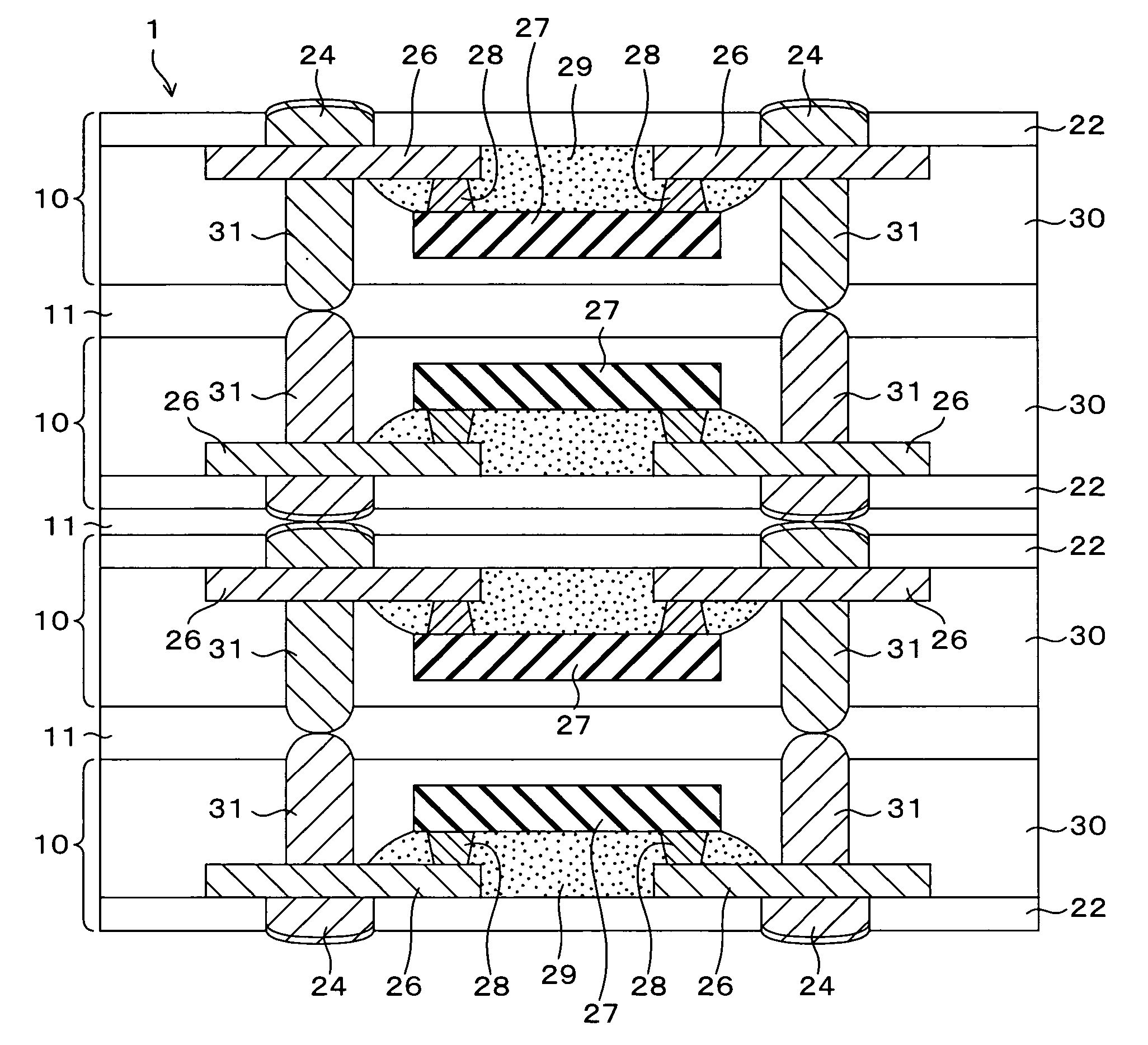
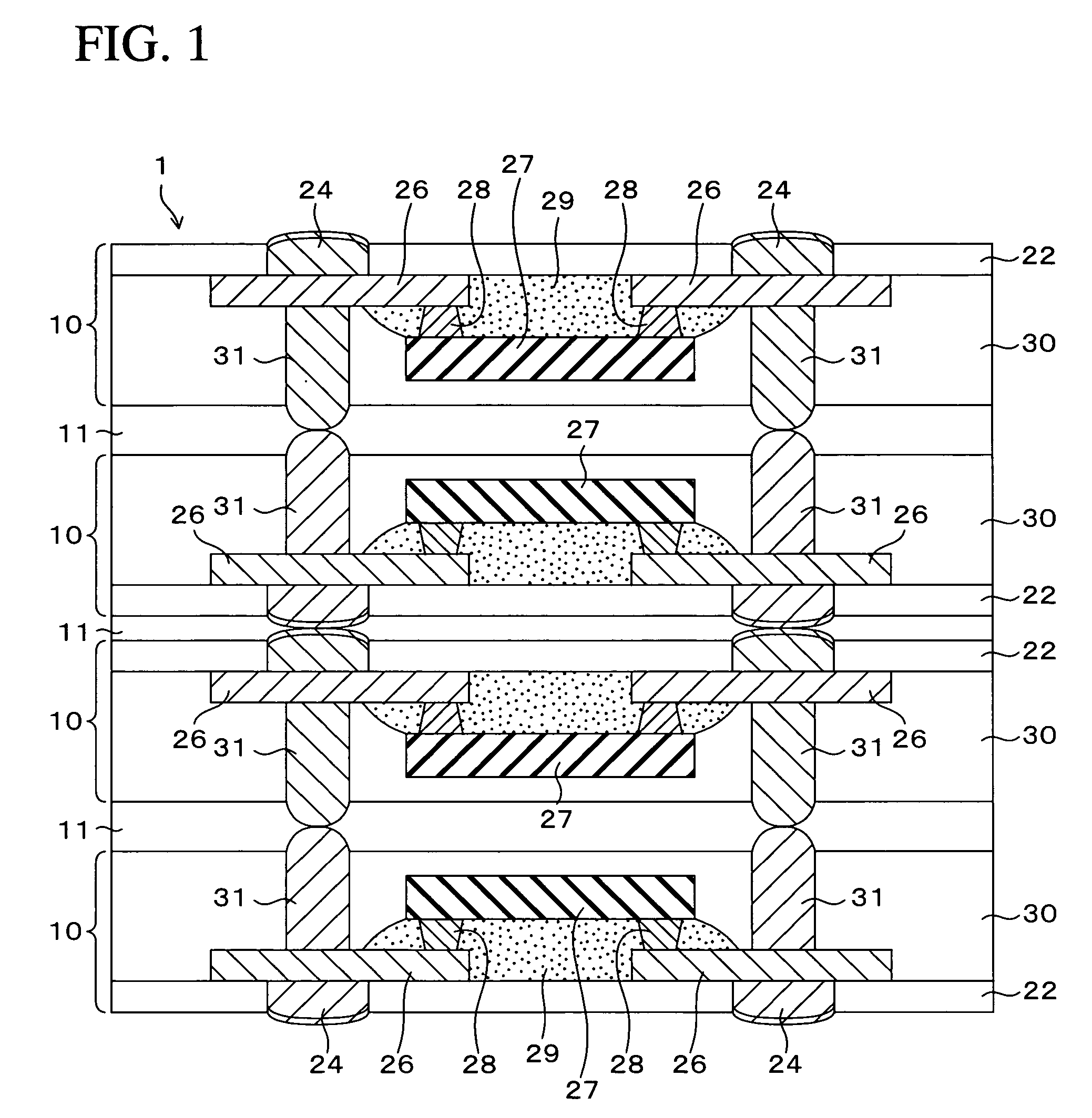
[0039]FIG. 1 is a sectional view showing an electronic parts packaging structure according to a first embodiment of the present invention.

[0040] An electronic parts packaging structure (semiconductor device) 1 of the present embodiment has a structure that plural (four in FIG. 1) sheet(thin film)-like units 10 are stacked to put an insulating layer 11 between them. Each unit 10 is constructed by a insulating resin layer (second insulating layer) 30, a semiconductor chip (electronic parts) 27 buried in the insulating resin layer 30, a solder resist layer (first insulating layer) 22, wirings 26, terminals 24, and contact vias 31. A thickness of one unit 10 is almost 200 μm (almost 100 to 300 μm), for example, and neighboring units 10 in the vertical direction (thickness direction) are electrically connected mutually via the terminals 24 or the contact vias 31 (connecting portions).

[0041] The electronic parts packaging structure 1 of the present embodiment ha...

second embodiment

[0071] (Second Embodiment)

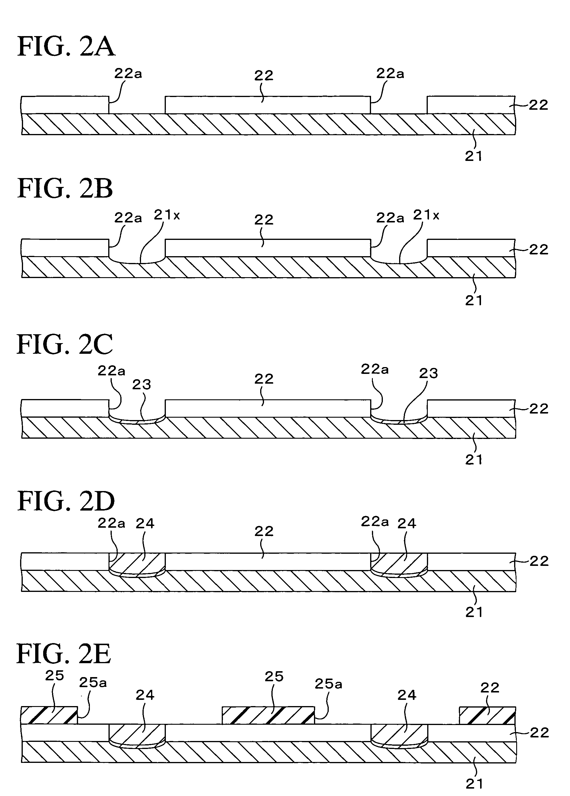
[0072]FIG. 4 is a sectional view showing a method of manufacturing an electronic parts packaging structure according to a second embodiment of the present invention, and FIG. 5 is a schematic plan view (general view) showing the same. In FIG. 4, the same reference symbols are affixed to the same constituent parts in FIG. 2N.

[0073] A difference of the present embodiment from the first embodiment is that an edge portion is left like a frame when the substrate 21 is removed by the etching. Since other configurations are basically similar to the first embodiment, explanation of redundant portions will be omitted herein.

[0074] In the first embodiment, in step shown in FIG. 2N, the substrate 21 is removed completely from the unit 10. As described above, since a plurality of units 10 are formed at the same time while using a sheet of substrate 21 in the first embodiment, it may be considered that, depending on the number of the units 10 formed simultaneously, th...

third embodiment

[0077] (Third Embodiment)

[0078]FIGS. 6A and 6B are sectional views showing a method of manufacturing an electronic parts packaging structure according to a third embodiment of the present invention.

[0079] A difference of the present embodiment from the first embodiment is that the solder resist layer 22 is also formed on the back surface (surface opposite to the semiconductor chip mounting surface) of the substrate 21. Since other configurations are basically similar to the first embodiment, explanation of redundant portions will be omitted herein.

[0080] In the present embodiment, as shown in FIG. 6A, the solder resist layer 22 is formed on both surfaces of the substrate 21. Then, like the first embodiment, as shown in FIG. 6B, the terminals 24 and the wirings 26 are formed and the semiconductor chip 27 is mounted on the wirings 26. Then, the underfill 29 is filled between the semiconductor chip 27 and the wirings 26 and the solder resist layer 22, then the insulating resin layer ...


PUM

PropertyMeasurementUnit
thicknessaaaaaaaaaa
thicknessaaaaaaaaaa
thicknessaaaaaaaaaa

Abstract

In an electronic parts packaging structure of the present invention constructed by stacking a plurality of sheet-like units in a thickness direction, each of the units includes a first insulating layer, wirings formed on one surface of the first insulating layer, a semiconductor chip (electronic parts) connected to the wirings, a second insulating layer formed on an one surface side of the first insulating layer to cover the semiconductor chip, and connecting portions (terminals and contact vias) for connecting electrically the wirings and wirings of other unit, wherein arrangement of the first insulating layer, the semiconductor chip, the wirings, and the second insulating layer is symmetrical between units adjacent in a thickness direction.

Description

CROSS-REFERENCE TO RELATED APPLICATIONS [0001] This application is based on and claims priority of Japanese Patent Application No. 2005-211938 filed on Jul. 21, 2005, and No. 2005-373859 filed on Dec. 27, 2005, the entire contents of which are incorporated herein by reference. BACKGROUND OF THE INVENTION [0002] 1. Field of the Invention [0003] The present invention relates to an electronic parts packaging structure and a method of manufacturing the same and, more particularly, an electronic parts packaging structure having a package structure in which electronic parts such as a semiconductor device (chip), and the like are mounted in an inside of a wiring substrate to attain a reduction in thickness and a method of manufacturing the same. [0004] 2. Description of the Related Art [0005] Improvements in the functions of the electronic parts are facilitated recently. The LSI (Large Scale Integrated Circuit) technology as the key technology makes progress steadily toward a higher speed ...

Claims


Application Information

Patent Timeline
Patent Type & Authority Applications(United States)
IPC IPC(8): H01L23/34
CPCH01L2224/73204Y10T29/49126H01L2924/01078H01L2924/01079H01L2924/15331H01L2924/30105H01L21/563H01L21/568H01L21/6835H01L23/3128H01L25/105H01L2224/16225H01L2224/32225H01L2924/3511H01L2924/01057Y10T29/49117Y10T29/49155Y10T29/49124H01L2924/10253H01L2225/1058H01L2225/1023H01L2924/00012H01L2924/00H01L2224/16238
Inventor GOMYO, TOSHIOTAKEUCHI, YUKIHARUTAKAYANAGI, HIDENORIYAMANO, TAKAHARU
Owner SHINKO ELECTRIC IND CO LTD
Why Eureka
Try Eureka