Optical device, image display device and head mounted display
- Summary
- Abstract
- Description
- Claims
- Application Information
AI Technical Summary
Benefits of technology
Problems solved by technology
Method used
Image
Examples
first embodiment
[0054] An embodiment of the present invention will be described as follows with reference to the attached drawings.
[0055] (1-1. Structure of an Image Display Device)
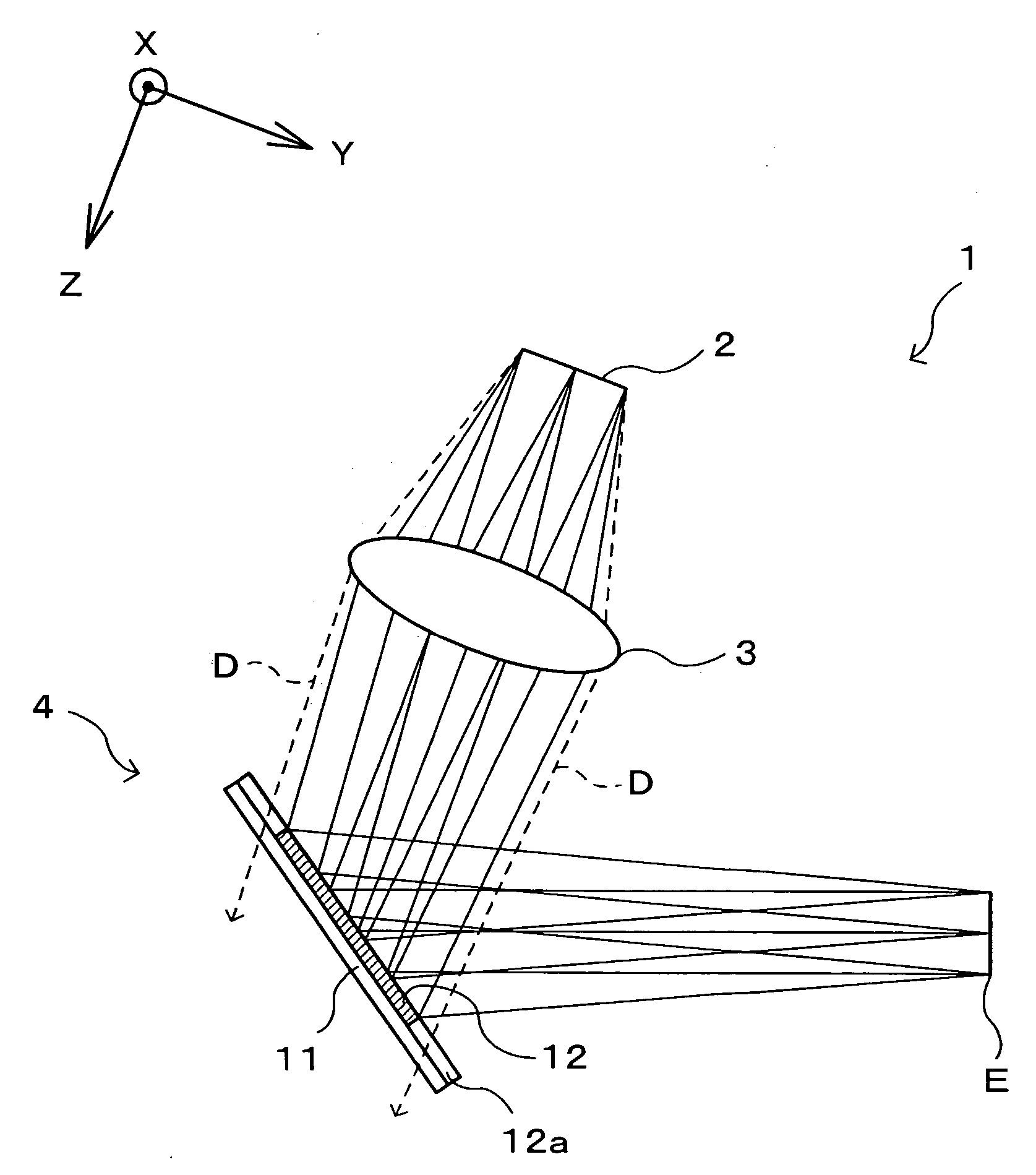
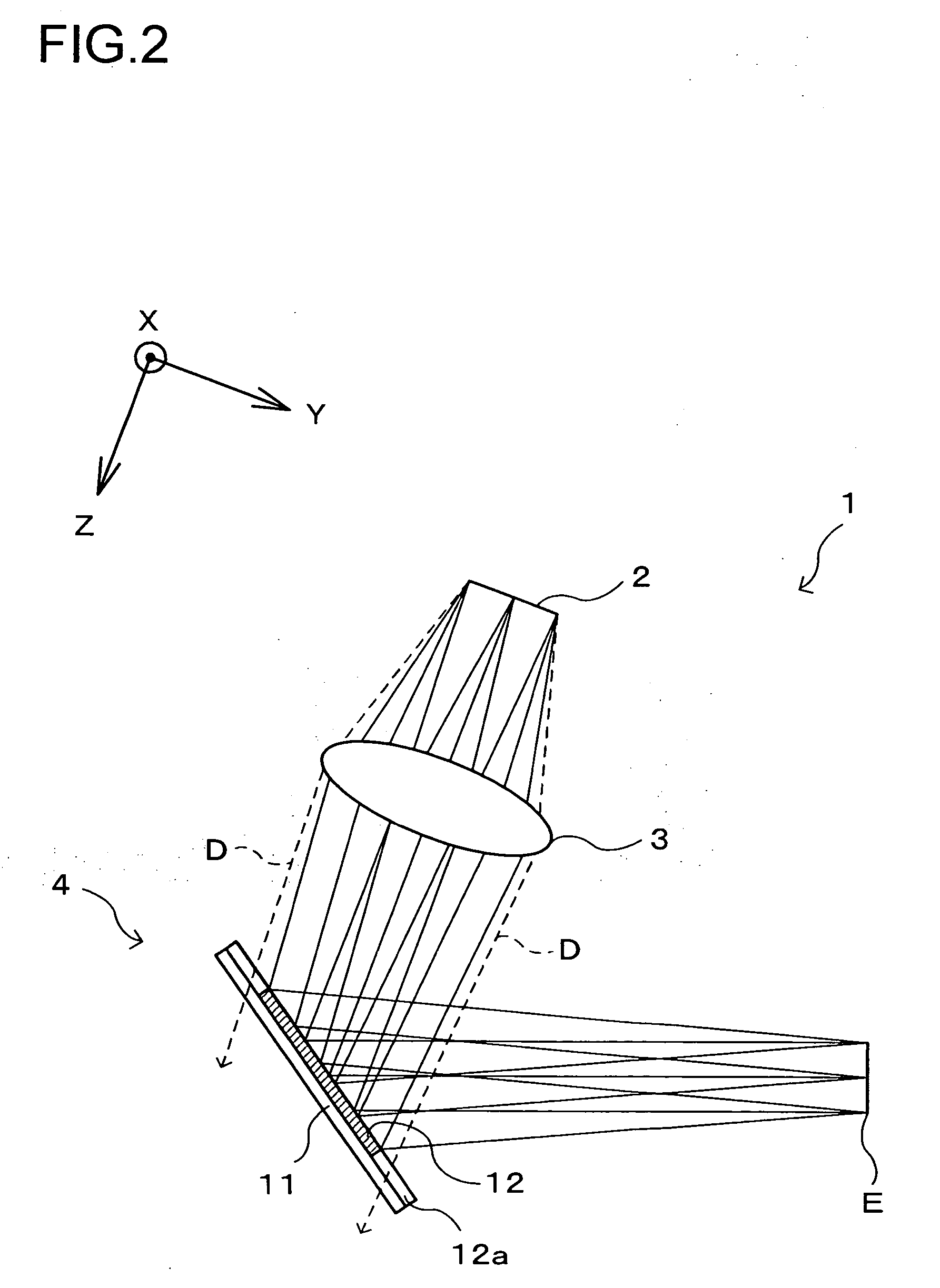
[0056]FIG. 2 is a cross section showing a general structure of the image display device 1 according to this embodiment. This image display device 1 includes a display element 2, an ocular lens 3 and an optical device 4.
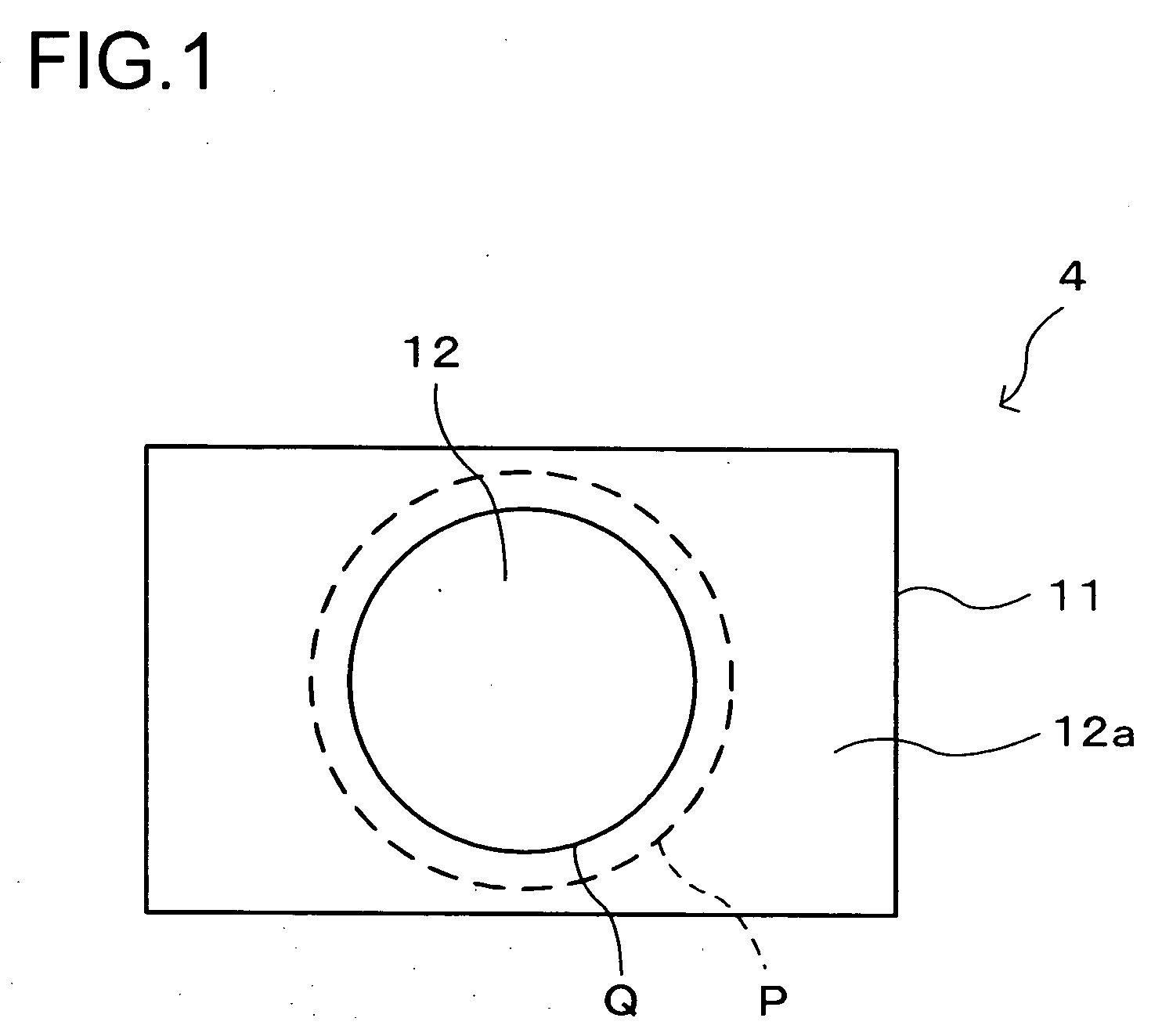
[0057] For convenience of description hereinafter, some directions are defined as follows. First, an optical axis is defined as an axis line connecting optically a center of a display area on the display element 2 with a center of an optical pupil E formed by the optical device 4. Then, a Z-direction is defined as a direction of the optical axis of an optical path from the display element 2 to the optical pupil E when it is developed. In addition, an X-direction is defined as a direction perpendicular to an incidence plane of the optical axis to a hologram optical element 12 of the optical device 4 that...
second embodiment
[0096] Another embodiment of the present invention will be described as follows with reference to the drawings. For convenience of description, the same elements as in the structure of the first embodiment are denoted by the same reference numerals, and descriptions thereof will be omitted.
[0097] (2-1. Structure of the Image Display Device)
[0098]FIG. 10 is a cross section showing a general structure of an image display device 1 according to the second embodiment, and FIG. 11 is an explanatory diagram showing an optical path in the image display device 1 in the state developed optically in one direction. This image display device 1 includes a display element 2 and an optical device 4.
[0099] The display element 2 includes a light source 13, a condensing lens 14 and a light modulation element 15. The light source 13 emits light that is supplied to the light modulation element 15. In this embodiment, particularly, the light source 13 is made up of a white color light source (a white ...
third embodiment
[0127] Still another embodiment of the present invention will be described as follows with reference to the drawings. For convenience of description, the same elements as in the structure of the first or the second embodiment are denoted by the same reference numerals, and descriptions thereof will be omitted.
[0128] (3-1. Structure of the Image Display Device)
[0129]FIG. 14 is a cross section showing a general structure of an image display device 1 according to this embodiment, and FIG. 15 is an explanatory diagram showing an optical path in the image display device 1 in the state developed optically in one direction. This image display device 1 includes a display element 2 and an optical device 4, and structures of the display element 2 and the optical device 4 are slightly different from those in the second embodiment.
[0130] The display element 2 includes a light source 13, a one-way diffuser plate 20, a condensing lens 14 and a light modulation element 15.
[0131] In this embodi...
PUM
 Abstract
Description
Claims
Application Information


