
Light-emitting module

a light-emitting module and light-emitting beam technology, applied in the field of light-emitting beams, can solve the problems of low light-emitting efficiency of light-emitted ball lenses, lack of light-emitting patterns, and increased costs, and achieve the effect of enhancing the use efficiency of light-emitted, without increasing the light-emitted laser beam amoun

Active Publication Date: 2007-01-25
FUJIFILM BUSINESS INNOVATION CORP
View PDF4 Cites 24 Cited by
  • Summary
  • Abstract
  • Description
  • Claims
  • Application Information

AI Technical Summary

Benefits of technology

[0010] The present invention has been made in view of the above circumstances and provides a light-emitting module that is capable of enhancing a use efficiency of the light emitted from the lens and monitoring a light amount of the laser beam without increasing the light amount of the emitted laser beam.

Problems solved by technology

When a light amount of the semiconductor light-emitting element is monitored, there is a disadvantage that a use efficiency of the light amount reflected by the ball lens is low.
If the laser light amount is increased to enter a light amount enough to operate the photo diode, which is not desirable in light of operating life and safety of the semiconductor light-emitting element such as VCSEL or the like.
In addition, the monitoring method described in Document 1 has to include the half mirror provided separately from the lens, leading to a problem of increased costs.
This completely lacks a light-emitting pattern, and this is not desirable in the optical communication.

Method used


Image

  • Light-emitting module
  • Light-emitting module
  • Light-emitting module

Examples


embodiments

(Embodiments)

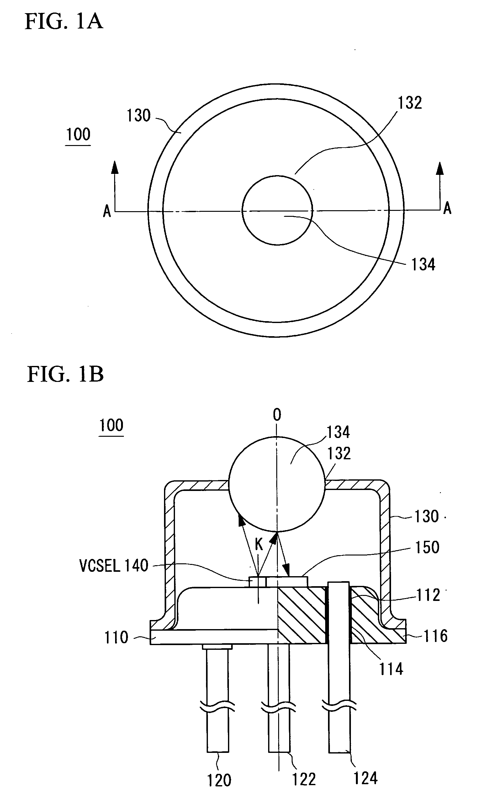
[0039]FIGS. 1 A and 1B are cross-sectional views showing a schematic configuration of a light-emitting module in accordance with a first embodiment of the present invention. A light-emitting module 100 in accordance with the present embodiment includes a metal stem 110, multiple lead pins 120, 122, and 124, and a metal cap 130. The metal stem 110 mounts a VCSEL chip. The multiple lead pins 120, 122, and 124 protrude from a backside of the stem 110. The metal cap 130 is attached to the stem 110.

[0040] Through holes 112 are provided in the stem 110 to attach the multiple lead pins 120, 122, and 124. An insulating film 114 is filled in an inner surface of the through hole 112 in order to electrically insulate the lead pins 120, 122, and 124 to be inserted. A VCSEL chip 140 and a semiconductor light-receiving element 150 of photo diode or the like, which is adjacently arranged thereto, are mounted on a plane of the stem 110. The lead pin 120 is an earth terminal and provid...


PUM


Abstract

A light-emitting module outputting laser beam emitted from a semiconductor light-emitting element via a lens, the light-emitting module includes a first main plane, a mount portion on the first main plane that mounts the semiconductor light-emitting element, a lens holding portion that holds the lens so that a light axis of the lens corresponds to a reference line crossed at right angles to the first main plane, a semiconductor light-receiving element that receives the laser beam reflected by the lens out of the laser beam emitted from the semiconductor light-emitting element. The semiconductor light-receiving element is positioned on the light axis of the lens and the semiconductor light-emitting element is provided away from the light axis of the lens.

Description

BACKGROUND OF THE INVENTION [0001] 1. Field of the Invention [0002] This invention relates to a light-emitting module that emits lights received from a semiconductor light-emitting element such as a semiconductor laser element or the like via a lens, and more particularly, to a technique of monitoring an optical output from the semiconductor light-emitting element. [0003] 2. Description of the Related Art [0004] A vertical cavity surface emitting laser diode (hereinafter referred to as VCSEL) is a laser diode that emits lights from a plane of a semiconductor substrate. VCSEL has several characteristics: VCSEL is lower in the drive current than that of an edge-emitting laser diode, the characteristic test can be performed at a wafer level, and can be readily produced into a two-dimensional array. Therefore, VCSEL is in use as a light source for optical information processing or optical communication, or as a light source of a data memory apparatus that stores data by means of light. ...

Claims


Application Information

Patent Timeline
Patent Type & Authority Applications(United States)
IPC IPC(8): H04B10/00H01S5/022
CPCG02B6/32H04B10/114H04B10/0799G02B6/4206
Inventor KUWATA, YASUAKINAKAYAMA, HIDEOMURAKAMI, AKEMIISHII, RYOJIMUKOYAMA, NAOTAKA
Owner FUJIFILM BUSINESS INNOVATION CORP
Learn More