Method of forming a layer and method of manufacturing a semiconductor device using the same

a manufacturing method and semiconductor technology, applied in the direction of crystal growth process, polycrystalline material growth, chemistry apparatus and processes, etc., can solve the problems of reducing the current drive capacity affecting the operation speed of the semiconductor device, and difficult forming of the pad, so as to reduce the damage to the lower structure formed on the semiconductor substrate, reduce the electrical resistance, and reduce the effect of impurity concentration

Inactive Publication Date: 2007-02-01
SAMSUNG ELECTRONICS CO LTD
View PDF5 Cites 13 Cited by
  • Summary
  • Abstract
  • Description
  • Claims
  • Application Information

AI Technical Summary

Benefits of technology

[0027] According to example embodiments of the present invention, a pad may have a multi-layered structure including a single crystalline silicon film doped with impurities and a polysilicon film doped with impurities on the single crystalline silicon film. Damages to lower structures formed on a semiconductor substrate may be diminished because the pad may be formed at a lower temperature of about 550° C. to about 600° C. In addition, the pad may be formed using amorphous silicon doped with impurities, and the pad having a higher concentration of impurities may be formed. Thus, the pad may have a reduced electrical resistance, and a. semiconductor device including the pad may have an improved operation speed and a reduced refresh failure.

Problems solved by technology

Forming a pad may be very difficult because the pad connecting isolated elements on a semiconductor substrate by using a highly conductive layer has become finer.
When the electrical resistance of the pad increases, current drive capacity of the semiconductor device may be reduced and thus operation speed of the semiconductor device may also be deteriorated.
Furthermore, a failure rate of refresh operation of the semiconductor device may increase.
Therefore, an additional process for removing the native oxide layer frequently formed on a substrate may be disadvantageously performed.
However, the SEG process may damage semiconductor elements disposed on the substrate because the SEG process may be performed at a higher temperature above about 800° C. Thus, this process may deteriorate electrical characteristics of the semiconductor elements.
However, the concentration of the impurities in the pad formed by the SPE growth process may be so low that electric currents cannot flow through the pad.

Method used


Image

  • Method of forming a layer and method of manufacturing a semiconductor device using the same
  • Method of forming a layer and method of manufacturing a semiconductor device using the same
  • Method of forming a layer and method of manufacturing a semiconductor device using the same

Examples


Embodiment Construction

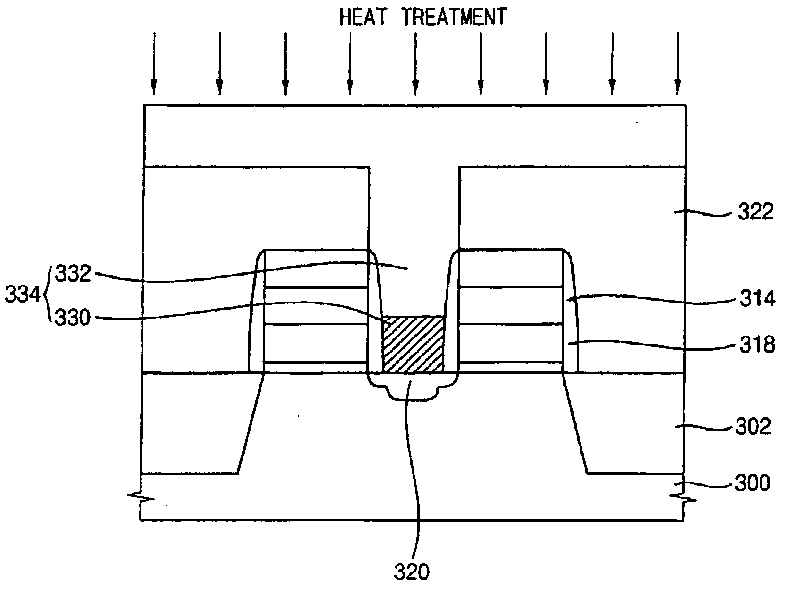
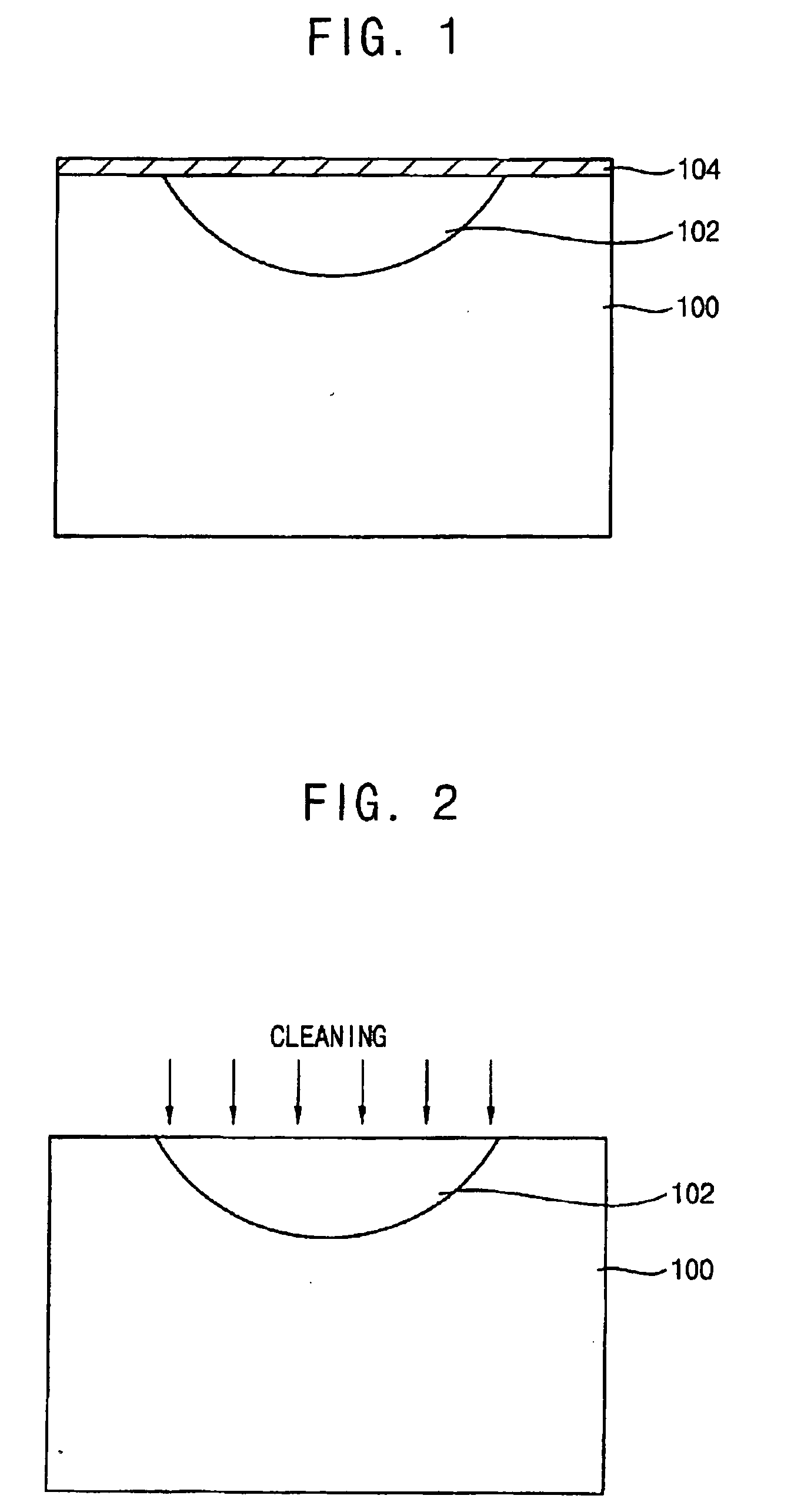
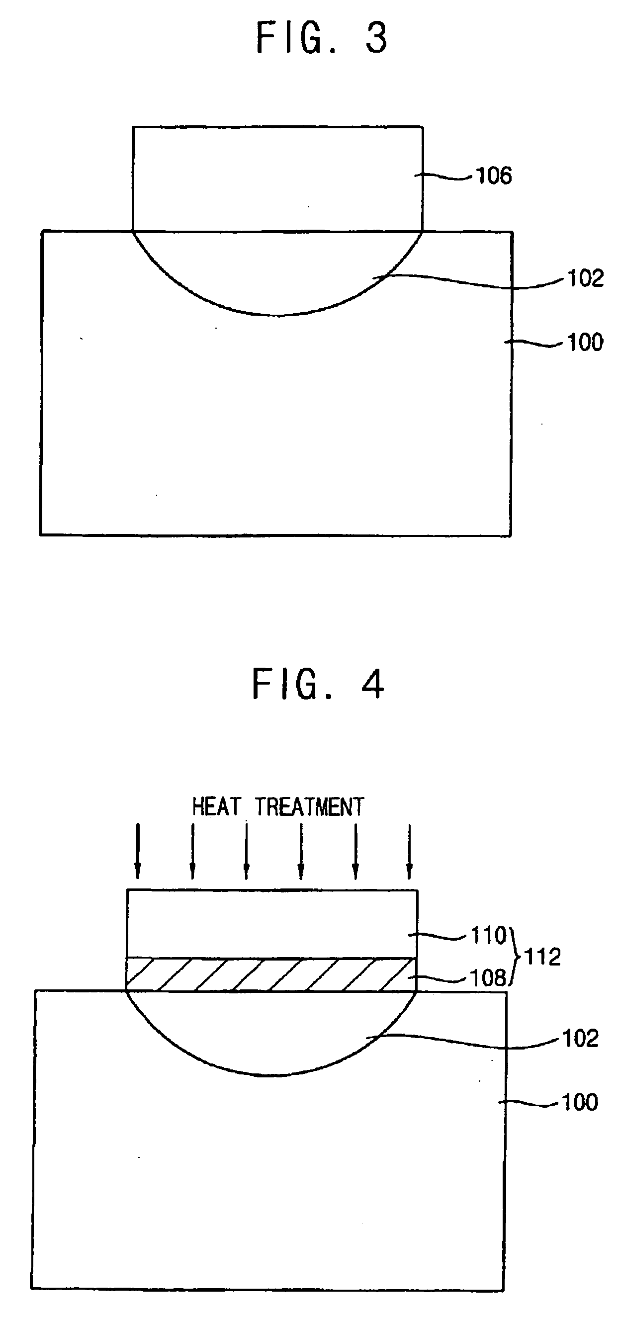
[0033] Example embodiments of the present invention are described more fully hereinafter with reference to the accompanying drawings, in which example embodiments of the present invention are shown. The present invention may, however, be embodied in many different forms and should not be construed as limited to the example embodiments set forth herein. Rather, these example embodiments are provided so that this disclosure will be thorough and complete, and will fully convey the scope of the present invention to those skilled in the art. In the drawings, the sizes and relative sizes of layers and regions may be exaggerated for clarity.

[0034] It will be understood that when an element or layer is referred to as being “on,”“connected to” or “coupled to” another element or layer, it can be directly on, connected or coupled to the other element or layer or intervening elements or layers may be present. In contrast, when an element is referred to as being “directly on,”“directly connecte...


PUM

PropertyMeasurementUnit
temperatureaaaaaaaaaa

Abstract

In a method of forming a layer having a lower electrical resistance and a method of manufacturing a semiconductor device, a first layer may be formed on a single crystalline substrate using amorphous silicon doped with impurities. A heat treatment may be performed on the single crystalline substrate at a temperature of about 550° C. to about 600° C. to convert the first layer into a second layer including a single crystalline silicon film transformed from a lower portion of the first layer contacting the single crystalline substrate and a polysilicon film transformed from an upper portion of the first layer. The layer may be formed at a relatively low temperature by a selective epitaxial growth process, and thus degradation or damage to a semiconductor device, which may be generated in a high temperature process, may be reduced.

Description

PRIORITY STATEMENT [0001] This application claims priority under 35 USC. §119 to Korean Patent Application No. 10-2005-69355 filed on Jul. 29 2005, the contents of which are herein incorporated by reference in their entirety. BACKGROUND OF THE INVENTION [0002] 1. Field of the Invention [0003] Example embodiments of the present invention relate to a method of forming a layer and a method of manufacturing a semiconductor device using the same. Example embodiments relate to a method of manufacturing a semiconductor device including a pad for electrically connecting a capacitor or a bit line to a source / drain region of a semiconductor substrate. [0004] 2. Description of the Related Art [0005] As semiconductor devices have become more integrated and operation speeds of semiconductor devices have become faster, demand for forming finer patterns has increased. Accordingly, a width of a wiring and a distance between wirings have been remarkably reduced. Forming a pad may be very difficult b...

Claims


Application Information

Patent Timeline
Patent Type & Authority Applications(United States)
IPC IPC(8): C30B15/14
CPCC30B29/06C30B1/023H01L21/20
Inventor PARK, JAE-YOUNGKIM, YOUNG-JINHYUNG, YONG-WOONAM, SEOK-WOOKIM, KYOUNG-SEOKYI, WOOK-YEOLLEAM, HUN-HYEOUNGLEE, KONG-SOOLEE, KO-EUN
Owner SAMSUNG ELECTRONICS CO LTD
Why Eureka
Try Eureka