Substrate based IC-package

Inactive Publication Date: 2007-02-01
POLARIS INNOVATIONS
View PDF4 Cites 3 Cited by
  • Summary
  • Abstract
  • Description
  • Claims
  • Application Information

AI Technical Summary

Benefits of technology

[0018] It is also possible to laminate a prepreg layer on both sides of the substrate. Thi

Problems solved by technology

But there is still a ring of solder mask on the side, which causes problems due to the uneven height of the solder mask ring (different bond line thickness).
The uneven distribution of the soldermask on the chipside and on the ballside of the substrate cause a high warpage of the substrate, whic

Method used


Image

  • Substrate based IC-package
  • Substrate based IC-package
  • Substrate based IC-package

Examples


Example

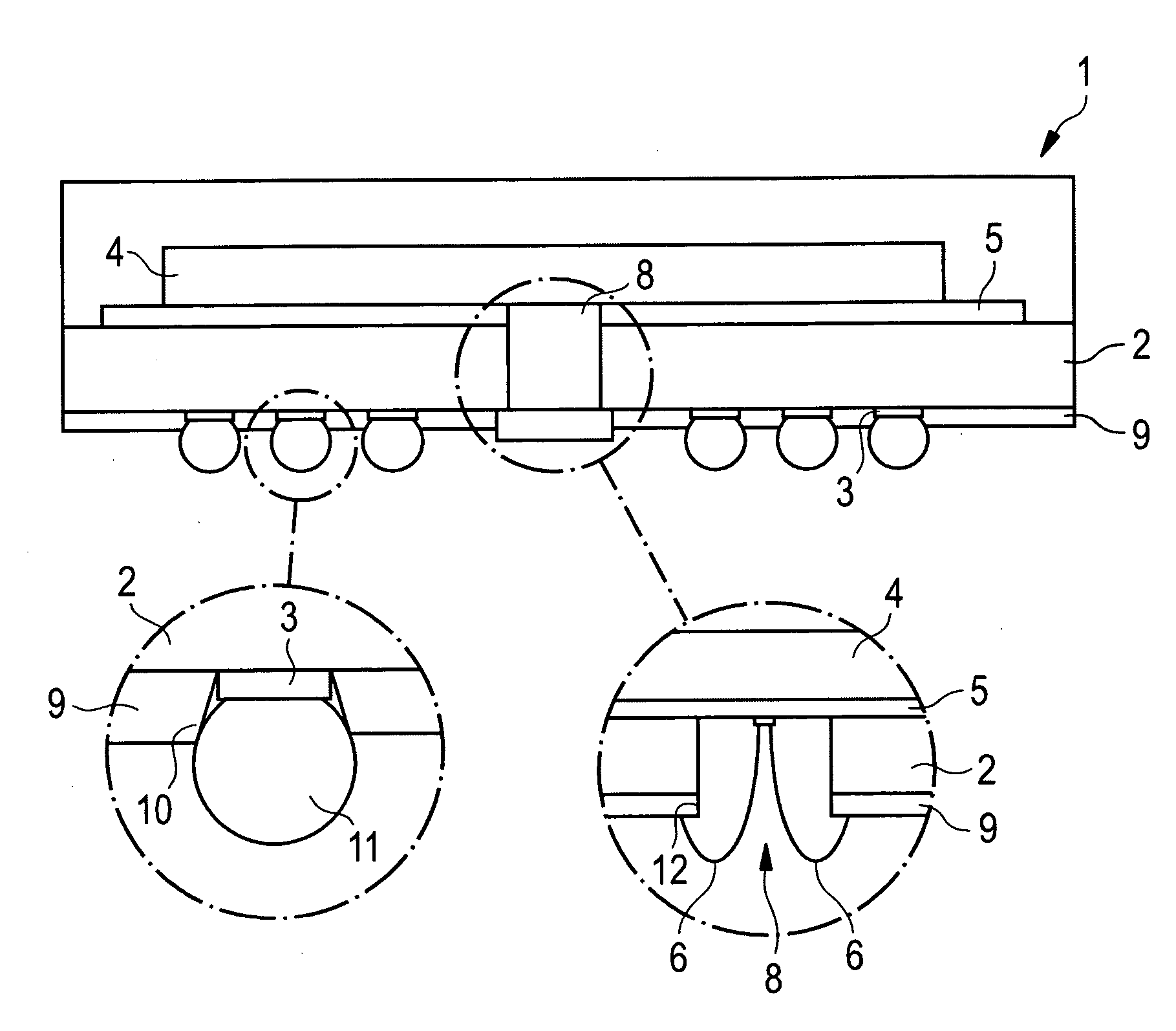
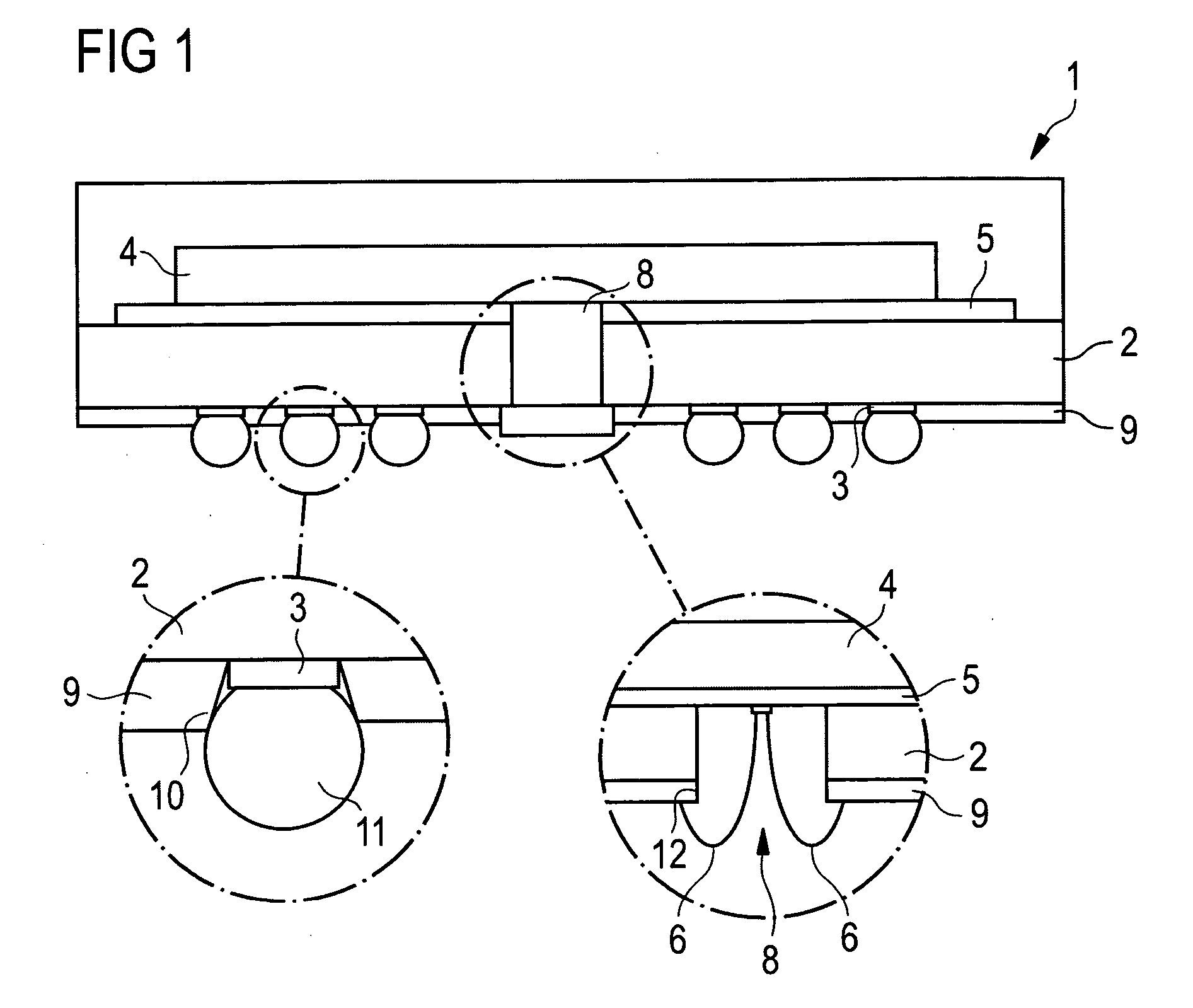
[0025] The making and using of the presently preferred embodiments are discussed in detail below. It should be appreciated, however, that the present invention provides many applicable inventive concepts that can be embodied in a wide variety of specific contexts. The specific embodiments discussed are merely illustrative of specific ways to make and use the invention, and do not limit the scope of the invention.

[0026] According to FIG. 1, the BOC (Board On Chip) package 1 includes a substrate 2 with contact pads 3 on one of its sides. The contact pads 3 are part of a not shown wiring on the substrate 2. The wiring is normally made of copper by a previous process. On the side opposite to the contact pads 3, a chip 4 is mounted with a die attach 5 between the substrate surface and the lower surface (active side of the chip) of the chip 4.

[0027] The chip 4 of this embodiment is provided with a central row of contact pads (not shown) which are connected via wire loops 6 with pads 7 o...


PUM


Abstract

A semiconductor component comprises a substrate that includes wiring on a first surface. A chip is mounted on a second surface of the substrate by a die attach, the second surface opposite the first surface. A bond channel in the center of the substrate allows for electrical connection of contact pads on the wiring with bond pads arranged in a center row on the chip by wire loops. A housing made of a mold compound surrounds a backside of the chip and parts of the substrate adjacent to the wiring. The semiconductor component further comprises a rigid prepreg layer covering, as well as the wiring of the substrate and the prepreg layer being provided with openings. Each opening is arranged in such a manner that the contact pads are accessible, and solder balls are mounted on each of the contact pads through the openings.

Description

TECHNICAL FIELD [0001] Generally to packaged integrated circuits and in more particular to a substrate based integrated circuit package. BACKGROUND [0002] An IC-package, such as a ball grid array package, includes a substrate having a first surface and a second surface. A chip is mounted on a surface and ball pads, conducting traces and solder masks on the other surface wherein the conducting traces are disposed in between the adjacent ball pads, and are covered by the solder mask. A portion of each of the ball pads is also covered by the solder mask. The solder mask is produced by photolithographic structuring and developing of an epoxy resin. [0003] The solder mask includes openings positioned in the area corresponding to the ball pads, wherein the opening exposes an opening of the surface of the substrate, the ball pad and a portion of the side wall of the wall pad. The chip is disposed on the second surface of the substrate and is sealed and encapsulated by the insulated materia...

Claims


Application Information

Patent Timeline
IPC IPC(8): H01L23/34H01L23/10
CPCH01L23/3114H01L2224/16225H01L23/49816H01L23/562H01L25/0657H05K3/281H05K3/3452H05K2201/09472H05K2201/09827H05K2203/0594H05K2203/063H01L24/48H01L2224/16227H01L2224/4824H01L2924/1434H01L2924/1436H01L2924/15311H01L2225/06565H01L23/3128H01L2924/14H01L2924/00014H01L2924/00H01L2224/45099H01L2224/45015H01L2924/207
Inventor REISS, MARTINNOCKE, KERSTIN
Owner POLARIS INNOVATIONS
Why Eureka
Try Eureka