Bonding pad fabrication method, method for fabricating a bonding pad and an electronic device, and electronic device

a fabrication method and bonding pad technology, applied in the direction of conductive pattern formation, sustainable manufacturing/processing, final product manufacturing, etc., can solve the problems of difficult uniform force to apply preventing the wire from being properly connected to the bonding pad, and requiring mask alignment work on each substrate. , to achieve the effect of easy fabrication, easy formation of bonding pad, and simplified fabrication method

Inactive Publication Date: 2007-02-01
SEIKO EPSON CORP
View PDF10 Cites 18 Cited by
  • Summary
  • Abstract
  • Description
  • Claims
  • Application Information

AI Technical Summary

Benefits of technology

[0008] An advantage of the invention is to provide a bonding pad fabrication method by which a bonding pad can easily be fabricated. Another advantage of the invention is to provide a method for fabricating a bonding pad of good bonding nature and an electronic device. Yet another advantage of the invention is to provide an electronic device.
[0009] According to a first aspect of the invention, a bonding pad fabrication method for forming a pad on a substrate includes disposing a droplet including a liquid containing a conductive material on the substrate by a droplet ejection method and forming the pad by solidifying the disposed droplet.
[0010] According to the first aspect of the invention, it is possible to easily form a bonding pad by disposing a droplet including a liquid containing a conductive material on a substrate and then solidifying the disposed droplet. Because this method requires no mask alignment unlike a thin film formation method, the fabrication method can be simplified.
[0011] It is preferable that the pad be formed in a cylindrical shape in the pad forming step of the bonding pad fabrication method according to the first aspect of the invention.
[0012] According to the first aspect of the invention, the cylindrical bonding pad requires less material to form than a hexahedron bonding pad. This is because if the diameter of a circular cross section of the cylindrical pad, is identical in size to one edge of a rectangular cross section of the hexahedron pad, the area of the circle is smaller than that of the rectangle.
[0013] In this case, the pad may be formed in a concave shape in the pad forming step of the bonding pad fabrication method according to the first aspect of the invention.

Problems solved by technology

It is troublesome that each substrate requires mask alignment work.
The flat bonding pad makes it difficult to apply force to the pad uniformly when bonding a wire to the pad.
This may prevent the wire from being properly connected to the bonding pad.

Method used


Image

  • Bonding pad fabrication method, method for fabricating a bonding pad and an electronic device, and electronic device
  • Bonding pad fabrication method, method for fabricating a bonding pad and an electronic device, and electronic device
  • Bonding pad fabrication method, method for fabricating a bonding pad and an electronic device, and electronic device

Examples


embodiment

[0053] Embodiment

Bonding Pad Fabrication Method

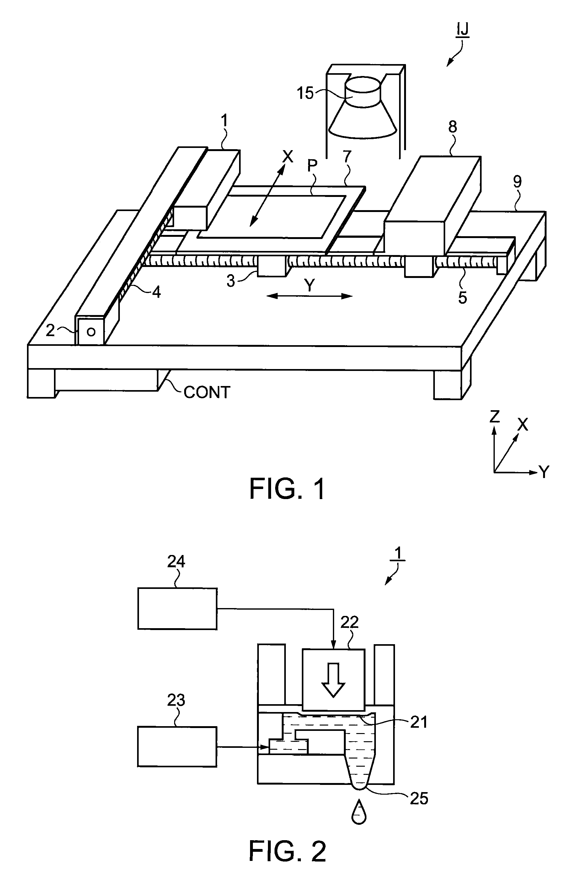
[0054] A method for forming a bonding pad according to this embodiment will now be described. In this embodiment, description is made on a method for forming a cylindrical bonding pad by ejecting a droplet including a conductive material in a droplet shape from an ejection nozzle of a droplet ejection head by a droplet ejection method, disposing the ejected droplet on a substrate subjected to surface treatment, and then solidifying the disposed droplet to form a cylindrical bonding pad.

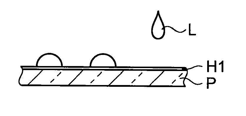
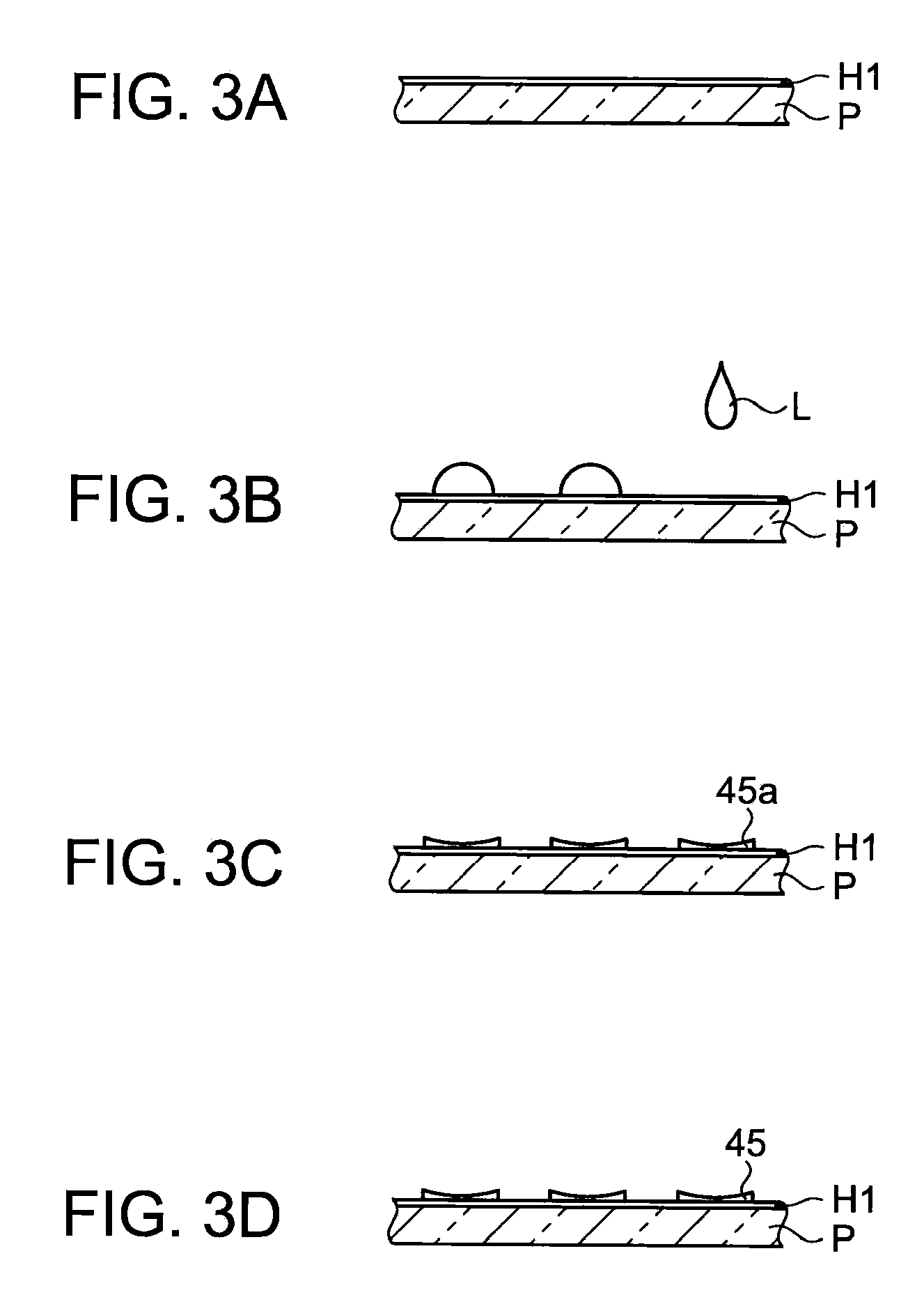
[0055]FIGS. 3A to 3D are process cross-sectional views showing the fabrication process of a bonding pad 45 according to this embodiment. FIG. 4 is a schematic flow chart showing the steps of the fabrication process of the bonding pad 45.

[0056] A method for fabricating a bonding pad 45 according to the invention is described referring to FIGS. 3 and 4. The method for forming a bonding pad 45 according to this embodiment generally includes a substrate c...

modification 1

[0079] Modification 1

[0080] In the above-mentioned embodiment, the cylindrical boding pad 45 having the concave part 47 is formed using the coffee stain phenomenon, but the invention is not limited to the embodiment. For example, the concave part 47 may not be formed on the bonding pad 45. Even though the bonding pad 45 without the concave part 47 is formed, the similar effect to that of the embodiment is achieved because the cylindrical bonding pad 45 is formed by the droplet ejection method.

modification 2

[0081] Modification 2

[0082] In the above-mentioned embodiment, Si having an insulative property is used as the material of the substrate P, but the invention is not limited to the embodiment. For example, it is possible to select a conductive material as the material of the substrate 9, dispose an insulating material by a droplet ejection method, and solidifying the disposed material. It is also possible to dispose an insulating film on a conductive substrate P and then form a bonding pad 45 on the substrate P. Even though the bonding pad 45 is formed in such a manner, the similar effect to that of the embodiment is achieved because the cylindrical bonding pad 45 is formed by the droplet ejection method.


PUM


Abstract

A method for fabricating a bonding pad 45 includes disposing a droplet L including a liquid containing a conductive material on a substrate P by a droplet ejection method and solidifying the disposed droplet L to forms the pad. The bonding pad 45 formed has a cylindrical shape and includes a concave part 47.

Description

BACKGROUND [0001] 1. Technical Field [0002] The present invention relates to a bonding pad fabrication method, a method for fabricating a bonding pad and an electronic device, and an electronic device. [0003] 2. Related Art [0004] In a semiconductor device, a semiconductor device (chip) and a bonding pad as an electrode pad, both disposed on a substrate, are connected by a bonding wire. The bonding wire is made of a conductive material, such as aluminum or gold, and establishes continuity between the semiconductor device (chip) and the bonding pad. [0005] As described in an example below, the bonding pad is made of a conductive material, such as aluminum, and a thin film forming method is used because when forming a film, the method can easily control the thickness of the film. [0006] JP-A-2005-167274 is an example of related art. [0007] However, the method according to JP-A-2005-167274 requires more accurate mask alignment as the shape of the bonding pad becomes minuter. It is trou...

Claims


Application Information

Patent Timeline
Patent Type & Authority Applications(United States)
IPC IPC(8): H01L23/48
CPCH01L24/02H01L24/45H01L24/48H01L24/85H01L2224/0401H01L2224/04042H01L2224/45124H01L2224/45139H01L2224/45144H01L2224/45147H01L2224/48091H01L2224/48227H01L2224/48475H01L2224/48599H01L2224/48699H01L2224/85051H01L2224/85205H01L2224/85385H01L2924/01002H01L2924/01004H01L2924/01005H01L2924/01006H01L2924/01007H01L2924/01013H01L2924/01014H01L2924/01015H01L2924/01018H01L2924/01022H01L2924/01025H01L2924/01028H01L2924/01029H01L2924/01033H01L2924/01042H01L2924/01046H01L2924/01047H01L2924/01049H01L2924/0105H01L2924/01051H01L2924/01054H01L2924/01074H01L2924/01077H01L2924/01078H01L2924/01079H01L2924/01082H01L2924/14H05K1/111H05K3/125H05K2201/09745H05K2203/013H01L2924/01024H01L2924/10253H01L2924/00014H01L2924/00H01L2924/12044H01L2224/48472H01L2924/10161H01L2224/85444H01L2224/85423Y02P70/50H01L2924/00015H01L2224/4554H01L2224/45015H01L2924/207H01L23/48H05K3/12H01L2224/05554
Inventor TOYODA, NAOYUKI
Owner SEIKO EPSON CORP
Why Eureka
Try Eureka