
All MOS power-on-reset circuit

a technology of power-on-reset circuit and all-mos, which is applied in the direction of pulse automatic control, pulse technique, electronic switching, etc., can solve the problems of occupying too much space for the realization of such high time constants on the chip, and the general rise rate of the power supply, etc., and achieves the effect of small area

Inactive Publication Date: 2007-02-01
STANDRD MICROSYSTEMS CORPORATION
View PDF77 Cites 10 Cited by
  • Summary
  • Abstract
  • Description
  • Claims
  • Application Information

AI Technical Summary

Benefits of technology

[0011] Thus, various embodiments of the invention may provide a means for designing and building a reliable integrated POR circuit with a compact and small area. In one set of embodiments, the POR circuit comprises NMOS and PMOS devices, where a combination of the respective threshold voltages of the NMOS and PMOS devices is used to set the power-on-reset threshold.

Problems solved by technology

One problem of integrating a POR circuit according to this technique is with the rate of rise of the power supply, which is generally quite slow.
Realization of such high time constants on chip may take up too much space to be practical, although the same time constant may be easily realized in an external circuit.
Consequently, many integrated POR circuits feature metal oxide semiconductor (MOS) devices, which can be very small in size, coupling to some very large resistors that may consume excessively large semiconductor die areas.

Method used


Image

  • All MOS power-on-reset circuit
  • All MOS power-on-reset circuit
  • All MOS power-on-reset circuit

Examples


Embodiment Construction

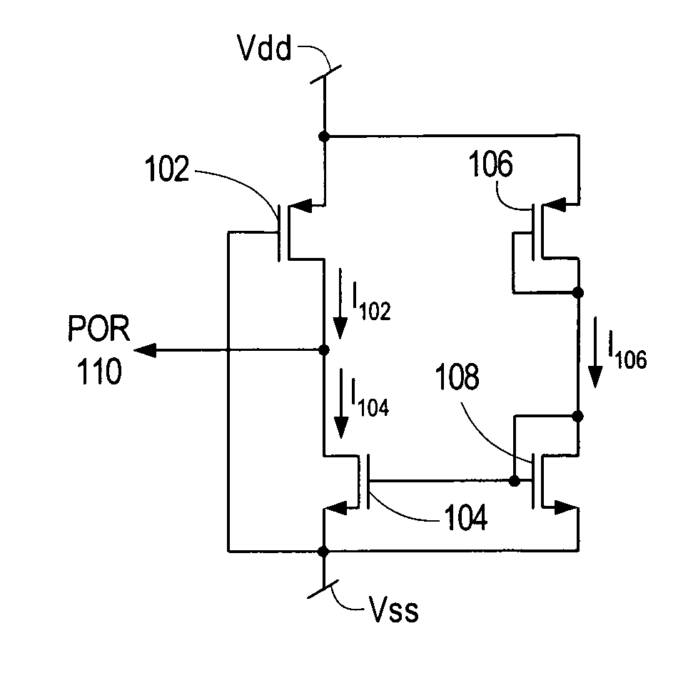
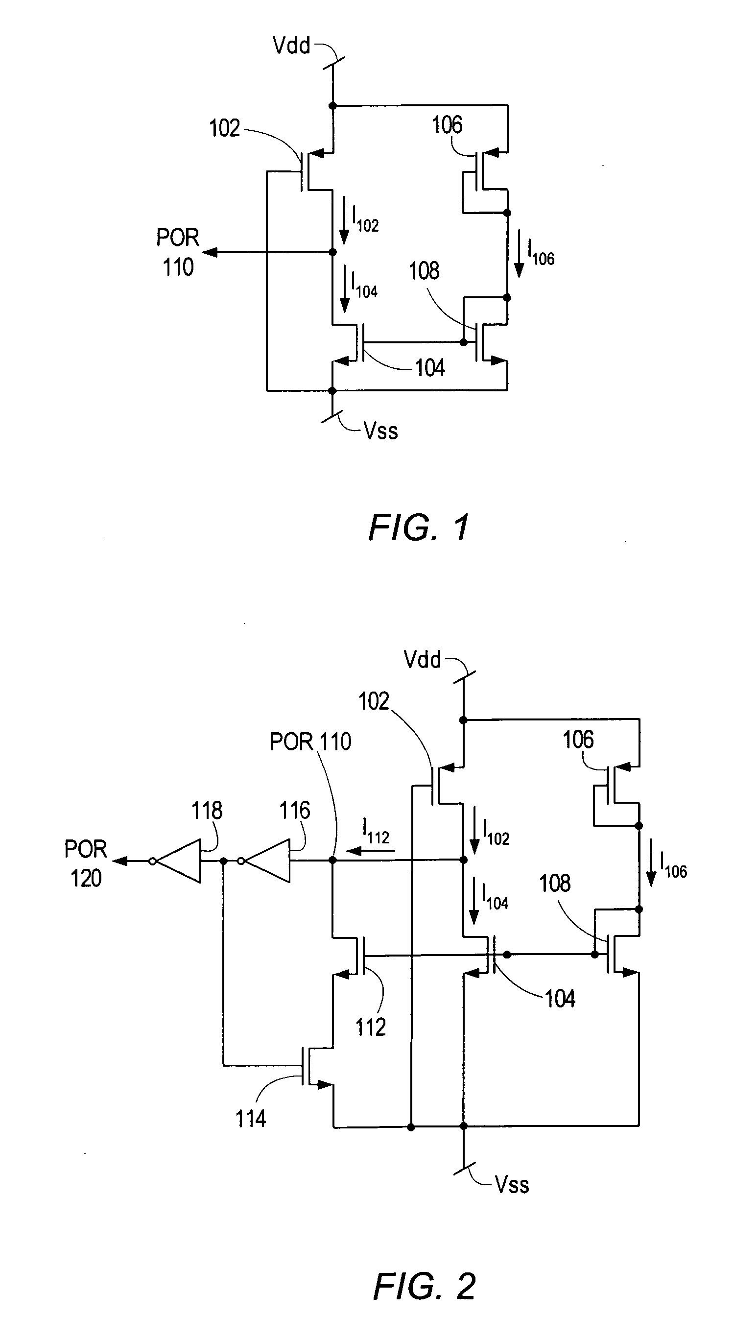
[0016] As used herein, the numeric subscript of a particular variable and / or parameter in equations (1) through (29) identifies the identically numbered respective MOS device in FIG. 1 and / or FIG. 2, to which the particular variable and / or parameter corresponds.

[0017]FIG. 1 shows one embodiment of an accurate, low variation and compact size POR (power-on-reset) circuit that may be coupled to a voltage supply configured to provide supply voltage Vdd. The POR circuit may be constructed using NMOS (n-channel metal-oxide semiconductor) devices 104 and 108, and PMOS (p-channel MOS) devices 102 and 106. PMOS device 106 may be coupled in series to NMOS device 108, with the respective drain terminals of PMOS 106 and NMOS 108 coupled together. In one embodiment, a POR output 110 is generated from the drain terminal of PMOS 102 which is coupled to the drain terminal of NMOS 104, as shown. By coupling the drain terminal of PMOS 106 to its gate terminal, and the drain terminal of NMOS 108 to i...


PUM


Abstract

A reliable, integrated POR (power-on-reset) circuit with a compact and small area. In one set of embodiments, the POR circuit comprises NMOS and PMOS devices, where a combination of the respective threshold voltages of the NMOS and PMOS devices is used to set the POR threshold. The NMOS and PMOS devices may be coupled in a configuration resulting in a POR threshold that is a function of the PMOS threshold voltage and a scaled version of the NMOS threshold voltage. The scaling factor may be a function of the transconductance parameters of the NMOS and PMOS devices. Additional NMOS devices may be configured in the POR circuit to provide hysteresis functionality, with one of the NMOS devices coupling to one of the original NMOS devices. The scaling factor used in determining the POR threshold in case of a falling supply voltage may then be a function of the transconductance parameters of the original NMOS and PMOS devices and the additional NMOS device coupling to one of the original NMOS devices.

Description

BACKGROUND OF THE INVENTION [0001] 1. Field of the Invention [0002] This invention relates generally to the field of integrated circuit design and, more particularly, to the design of power-on-reset (POR) circuits. [0003] 2. Description of the Related Art [0004] A POR (power-on-reset) signal is typically required by digital circuits such as memory elements, flip-flops, microcontrollers and central processing units to set an initial state immediately after powering on the circuit. For example, when powered on, most of the programmed or programmable type logic circuits, in particular microprocessors, must be set in a zero state or RESET state in order to insure that no undetermined logic states are present in any portion of the circuit. This signal has been traditionally generated externally, typically using an external RC circuit or simply a switch, the latter having to be manually operated in most cases. [0005] More recently, integrated POR circuits have been incorporated into syste...

Claims


Application Information

Patent Timeline
IPC IPC(8): H03L7/00
CPCH03K17/223
Inventor MCLEOD, SCOTT C.
Owner STANDRD MICROSYSTEMS CORPORATION
Learn More