

Transparent conductive film for flat panel displays
a technology of transparent conductive film and flat panel display, which is applied in the direction of superimposed coating process, synthetic resin layered products, instruments, etc., can solve the problems of difficult control of chemical etching process, inability to manufacture such films by continuous process on flexible substrates, and inability to meet the requirements of continuous production, etc., to achieve high optical transmittance, low electrical resistance, and superior properties
- Summary
- Abstract
- Description
- Claims
- Application Information
AI Technical Summary
Benefits of technology
Problems solved by technology
Method used
Image

Examples
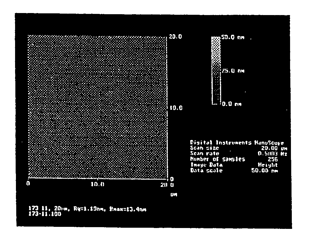
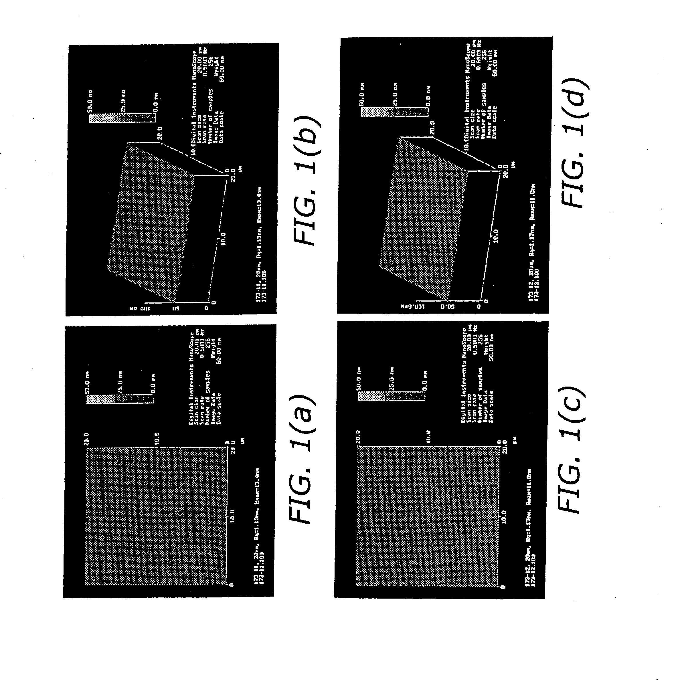
example 1
Roll-To-Roll Deposition and Characterization of ITO / APC / ITO Films
I. Deposition and Characterization
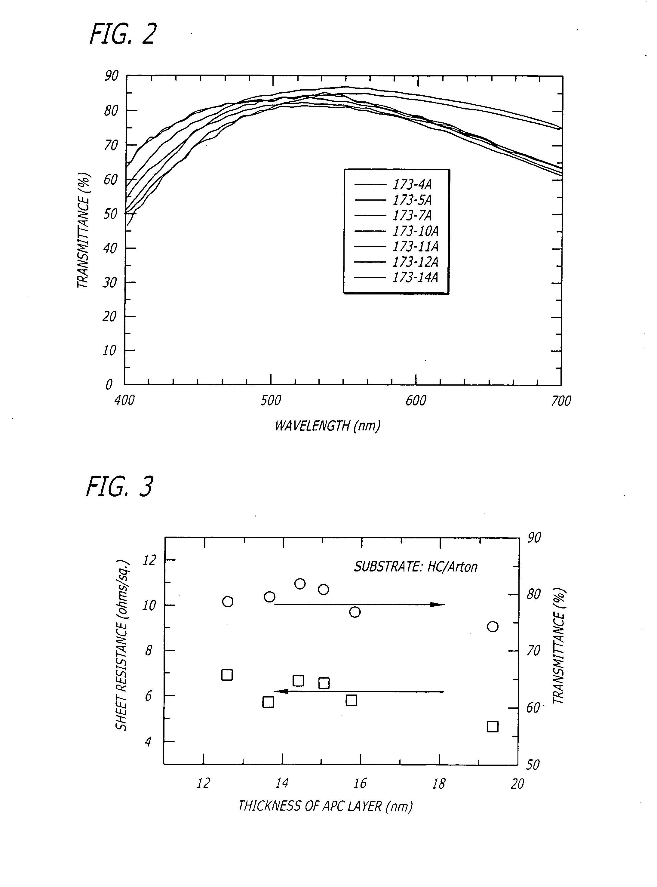
[0095] Substrate material was Lintec Arton coated with hard coating (HC / Arton). Table 1 lists the properties of the Lintec Arton. The hard coating on Lintec Arton has a surface composition of 35 at % C, 45 at % 0, and 20 at % Si, excluding hydrogen, and contains UV cured polyester acrylate and colloidal silica.
Properties of HC / Arton sheetSur-T %Thick-faceBarrierSurface(@Mate-nessRMSTg(g / m2 / day)energy550rialGRADE(μm)(nm)(C)(° C. / RH)(mN / M)nm)HC / CHC-1881.317131.436.391.4ArtonPN188W(40 / 100)(Lintec)PFW
[0096] Deposition experiments were carried out using Avery Sputtering System with the DC magnetron sputtering mode and the roll-to-roll substrate transportation.
[0097] The base pressure of the deposition chamber was 1.54×10⁻³ mT, and the working or deposition pressure was 2.4-3.1 mT. Prior to film deposition, the plastic roll was purged with Ar+O2 plasma to modify the surface chemistry o...
example 2
Roll-To-Roll Deposition and Characterization of ICO / APC / ICO Films
I. Deposition and Characterization
[0127] Substrate material was the Lintec Arton coated with hard coating (HC / Arton). The hard coating has a surface composition of 35 at % C, 45 at % 0, and 20 at % Si, excluding hydrogen, and contains uv cured polyester acrylate and colloidal silica. The properties of HC / Arton are listed in Table 1, above, in Example 1.
[0128] Deposition experiment was carried out using Avery Sputtering System with the DC magnetron sputtering mode and the roll-to-roll substrate transportation.
[0129] The base pressure of the deposition chamber was 1.5-4×10⁻³ mT, and the working or deposition pressure was 2.4-3.1 mT. Prior to film deposition, the plastic roll was purged with Ar+O2 plasma to modify the surface chemistry of plastic materials. The sputtering power of 1200 W and the gas flow-rate ratio of O2 / Ar of 5 / 50 sccm were used for the plasma purging.
[0130] An In2O3-10% CeO2 target was sputtered w...
PUM
| Property | Measurement | Unit |
|---|---|---|
| power | aaaaa | aaaaa |
| power | aaaaa | aaaaa |
| power | aaaaa | aaaaa |
Abstract
Description
Claims
Application Information