Metal pad or metal bump over pad exposed by passivation layer

a technology of passivation layer and metal pad, which is applied in the direction of semiconductor devices, semiconductor/solid-state device details, electrical devices, etc., can solve the problems of obstructing the high-speed operation of chips and only affecting good dies

Active Publication Date: 2007-02-01
QUALCOMM INC
View PDF25 Cites 63 Cited by
  • Summary
  • Abstract
  • Description
  • Claims
  • Application Information

AI Technical Summary

Problems solved by technology

Any problems in the wire bonding process thus impact only good die.
However, the high inductance cre...

Method used


Image

  • Metal pad or metal bump over pad exposed by passivation layer
  • Metal pad or metal bump over pad exposed by passivation layer
  • Metal pad or metal bump over pad exposed by passivation layer

Examples


Embodiment Construction

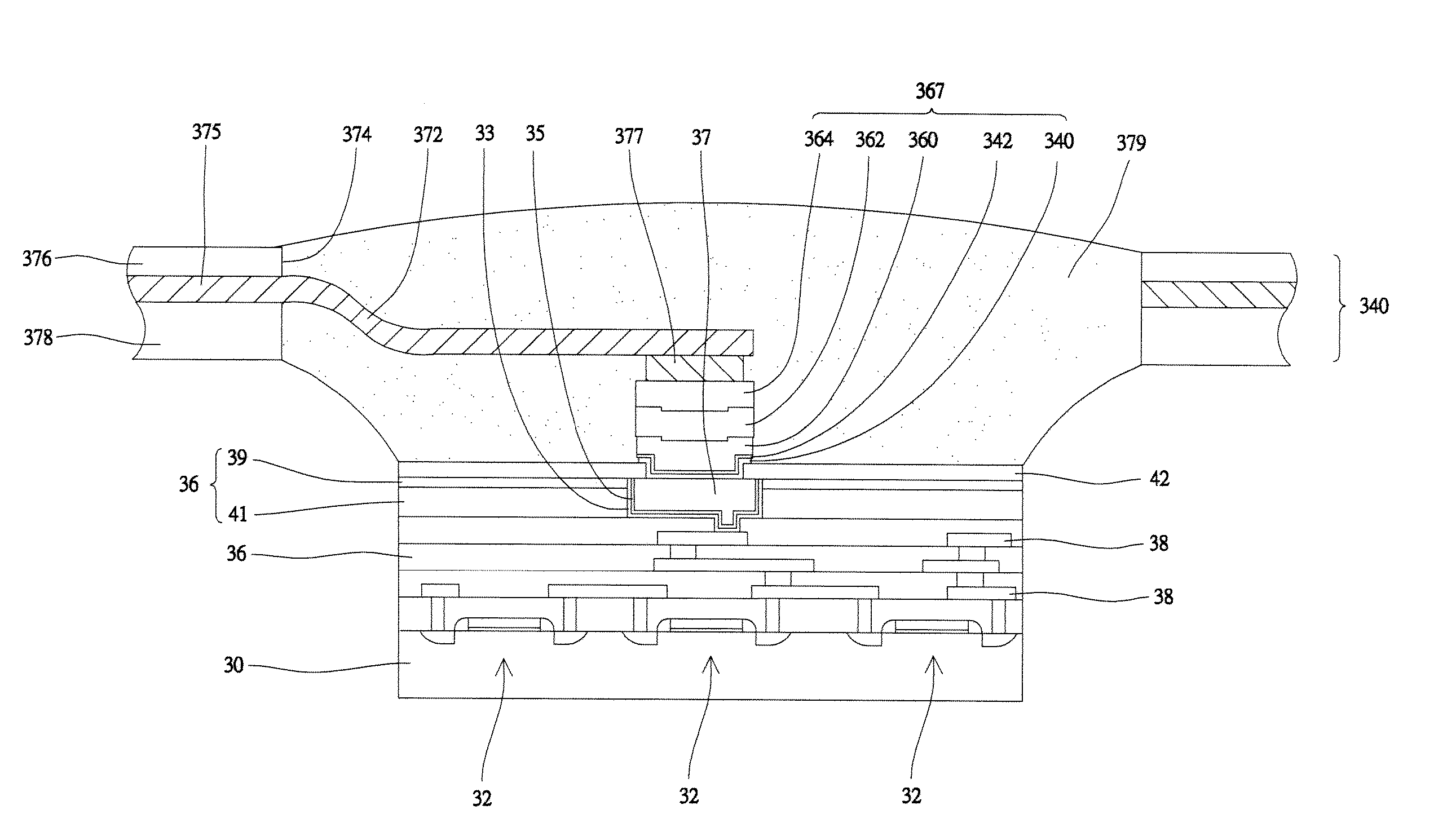
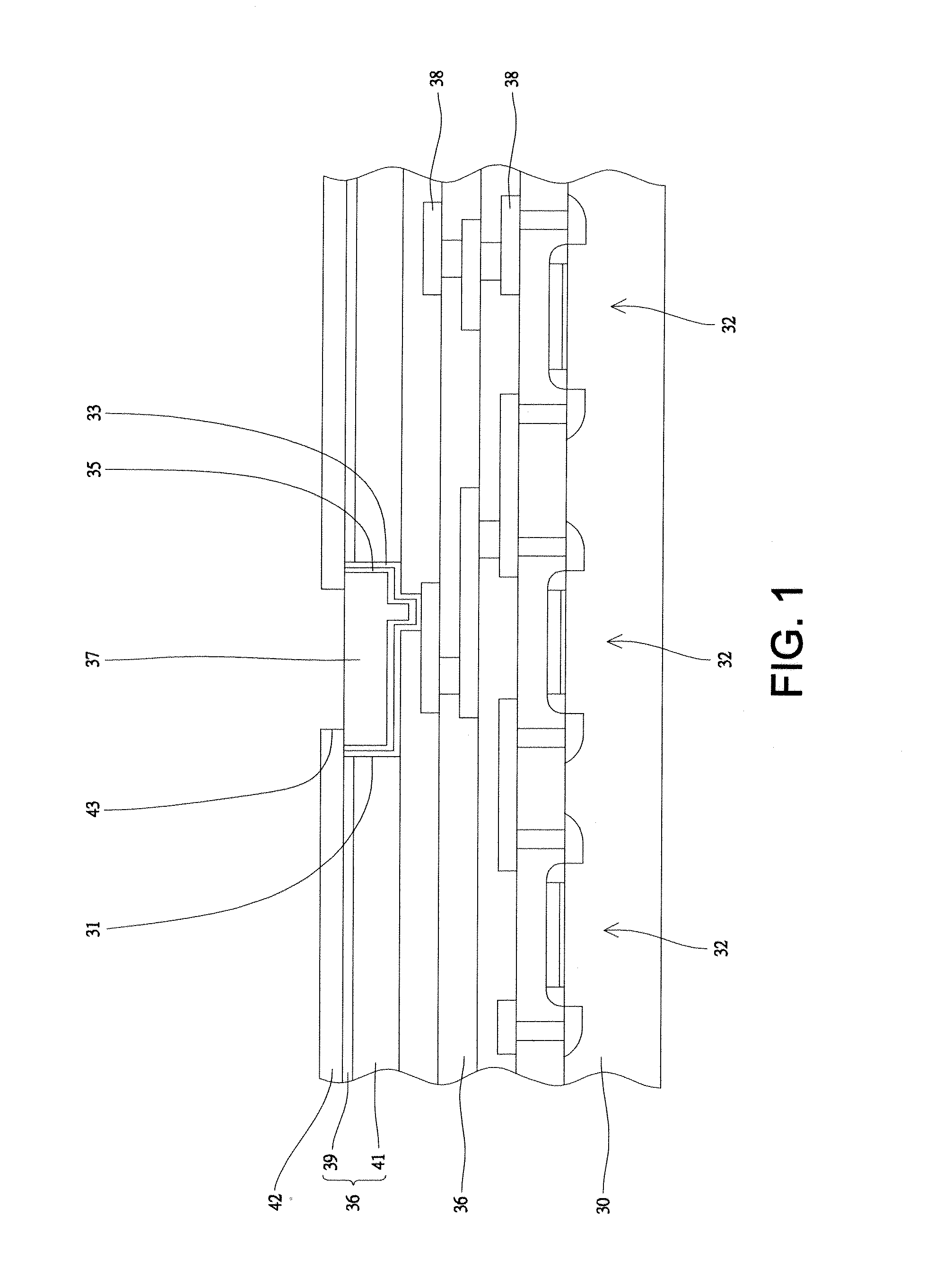
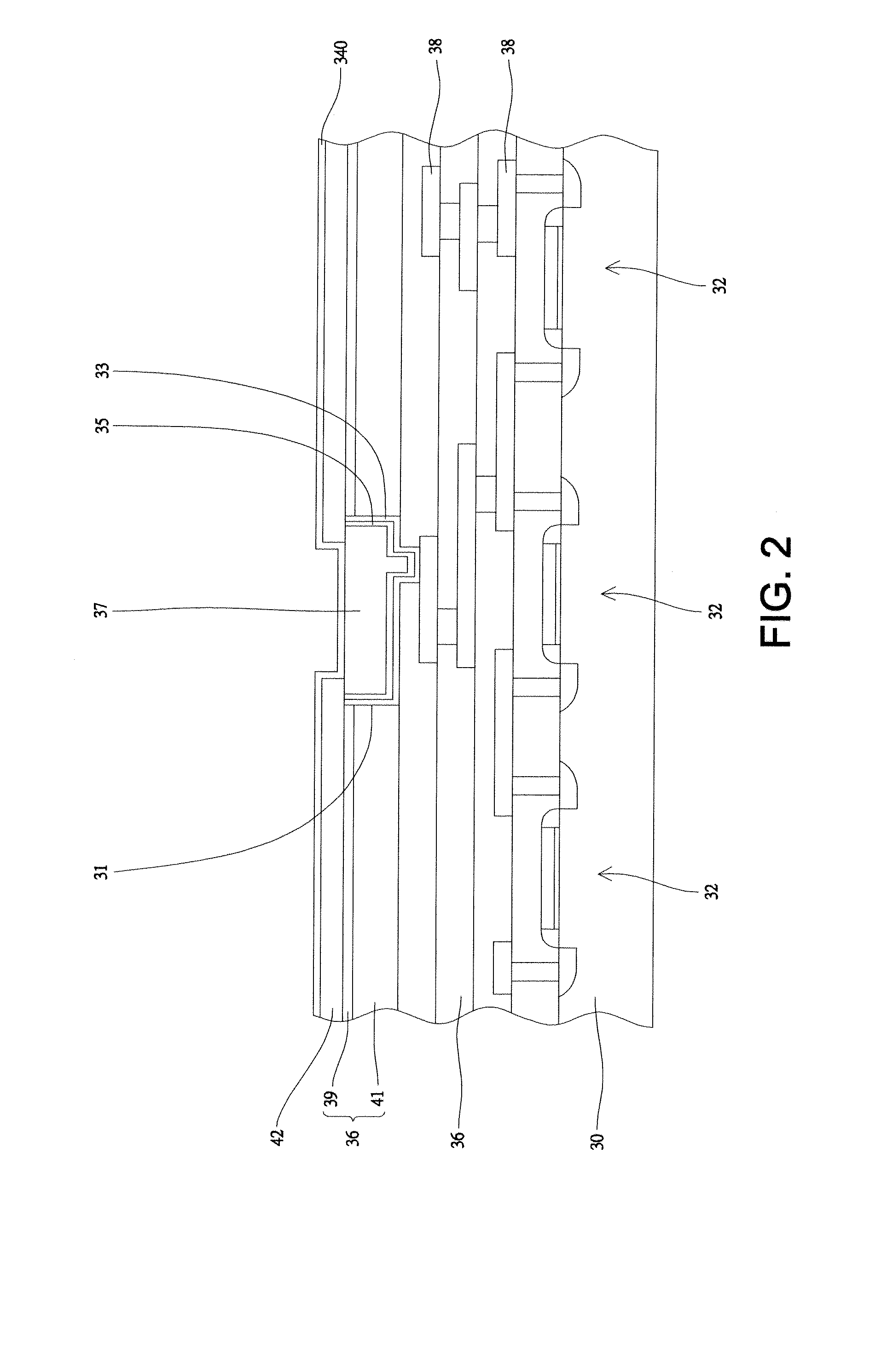
[0022] The following are the embodiments to illustrate the processes and structures to form a metallization structure, such as a metal bump or metal trace, over a copper pad on a semiconductor wafer. After the steps of forming metallization structure are finished, the semiconductor wafer is cut into multiple semiconductor chips for the following packaging processes.

[0023] Referring to FIG. 1, a semiconductor substrate 30 is provided, and the semiconductor substrate 30 may be Si substrate, GaAs substrate, GeSi substrate or SOI (silicon-on-insulator) substrate. The semiconductor substrate 30 is a circular semiconductor wafer. The semiconductor substrate 30 has an active surface having multiple electronic elements 32, which are formed via doping trivalent or pentavalent ions, such as boron ions or phosphorus ions. The electronic elements 32 may be MOS transistors, MOS devices, p-channel MOS devices, n-channel MOS devices, BiCMOS devices, Bipolar Junction Transistors, diffusion areas, ...


PUM


Abstract

A circuitry component comprising a semiconductor substrate, a pad over said semiconductor substrate, a tantalum-containing layer on a side wall and a bottom surface of said pad, a passivation layer over said semiconductor substrate, an opening in said passivation layer exposing said pad, a titanium-containing layer over said pad exposed by said opening, and a gold layer over said titanium-containing layer.

Description

[0001] This application claims priority to U.S. provisional application No. 60 / 703,932, filed on Jul. 29, 2005, and to U.S. provisional application No. 60 / 703,933, filed on Jul. 29, 2005, which are herein incorporated by reference in their entirety.BACKGROUND OF THE PRESENT INVENTION [0002] 1. Field of Invention [0003] The invention relates to a metallization structure over a semiconductor chip or wafer and the method for forming the same, and more particularly to a metallization structure over a copper pad and the method for forming the same. [0004] 2. Description of Related Arts [0005] The reduction of the feature sizes of semiconductor devices using state-of-the-art semiconductor techniques have dramatically increased the device packing density of a single integrated circuit (IC) chip. However, as the device packing density increases, it is necessary to increase the number of electrical metal interconnect layers on the IC chip to effectively wire up the discrete devices on a subs...

Claims


Application Information

Patent Timeline
IPC IPC(8): H01L21/76
CPCH01L2924/01006H01L2924/01007H01L2924/01011H01L2924/01013H01L2924/01014H01L2924/01015H01L2924/01022H01L2924/01027H01L2924/01028H01L2924/01029H01L2924/01046H01L2924/01047H01L2924/01049H01L2924/0105H01L2924/01073H01L2924/01074H01L2924/01075H01L2924/01078H01L2924/01079H01L2924/01082H01L2924/014H01L2924/04941H01L2924/04953H01L2924/05042H01L2924/10329H01L2924/14H01L2924/19041H01L2924/19042H01L2924/19043H01L2924/30107H01L23/3157H01L24/03H01L24/05H01L24/11H01L24/12H01L24/16H01L24/45H01L24/48H01L2224/02166H01L2224/0231H01L2224/0345H01L2224/0347H01L2224/0401H01L2224/04042H01L2224/04073H01L2224/05006H01L2224/05022H01L2224/05139H01L2224/05147H01L2224/05155H01L2224/05567H01L2224/05568H01L2224/05572H01L2224/05639H01L2224/05644H01L2224/05647H01L2224/05655H01L2224/05664H01L2224/05669H01L2224/05673H01L2224/05676H01L2224/05683H01L2224/1147H01L2224/11902H01L2224/11912H01L2224/13099H01L2224/45144H01L2224/48463H01L2924/01019H01L2924/01023H01L2924/01024H01L2924/01033H01L2924/01041H01L2924/01044H01L2924/01045H01L2224/48644H01L2224/48647H01L2224/48655H01L2224/48664H01L2224/48669H01L2224/48639H01L2224/48673H01L2224/48683H01L2924/13091H01L2924/0002H01L2924/1305H01L2924/00014H01L2924/00H01L2224/05552H01L2224/73204H01L2924/15787
Inventor LIN, MOU-SHIUNGLO, HSIN-JUNGCHOU, CHIU-MINGCHOU, CHIEN-KANGCHEN, KE-HUNG
Owner QUALCOMM INC
Why Eureka
Try Eureka