
High frequency semiconductor integrated circuit device, wireless electric unit and wireless communication system

a technology of integrated circuits and semiconductors, applied in the direction of waveguides, modulation devices, waveguide types, etc., to achieve the effects of reducing the number of parts of the system, reducing the amount of crosstalk, and reducing the number of parts

Inactive Publication Date: 2007-02-01
RENESAS ELECTRONICS CORP
View PDF9 Cites 11 Cited by
  • Summary
  • Abstract
  • Description
  • Claims
  • Application Information

AI Technical Summary

Benefits of technology

This configuration effectively suppresses coupling noise and crosstalk, enhancing the accuracy of power amplifier control and reducing the number of components, thereby improving packaging density and system efficiency.

Problems solved by technology

Therefore, in a system wherein a power amplifier and a high frequency IC are constituted of separate semiconductor chips, a problem arises: if a transmission oscillator is incorporated into the high frequency IC, the oscillation signal of the transmission oscillator is outputted from the external terminal of the high frequency IC to the power amplifier external to the chip.

Method used


Image

  • High frequency semiconductor integrated circuit device, wireless electric unit and wireless communication system
  • High frequency semiconductor integrated circuit device, wireless electric unit and wireless communication system
  • High frequency semiconductor integrated circuit device, wireless electric unit and wireless communication system

Examples


first embodiment

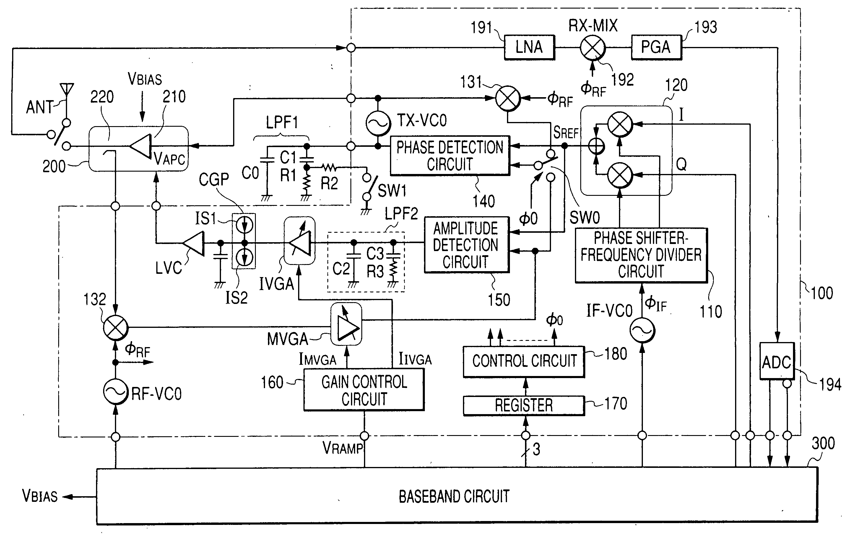
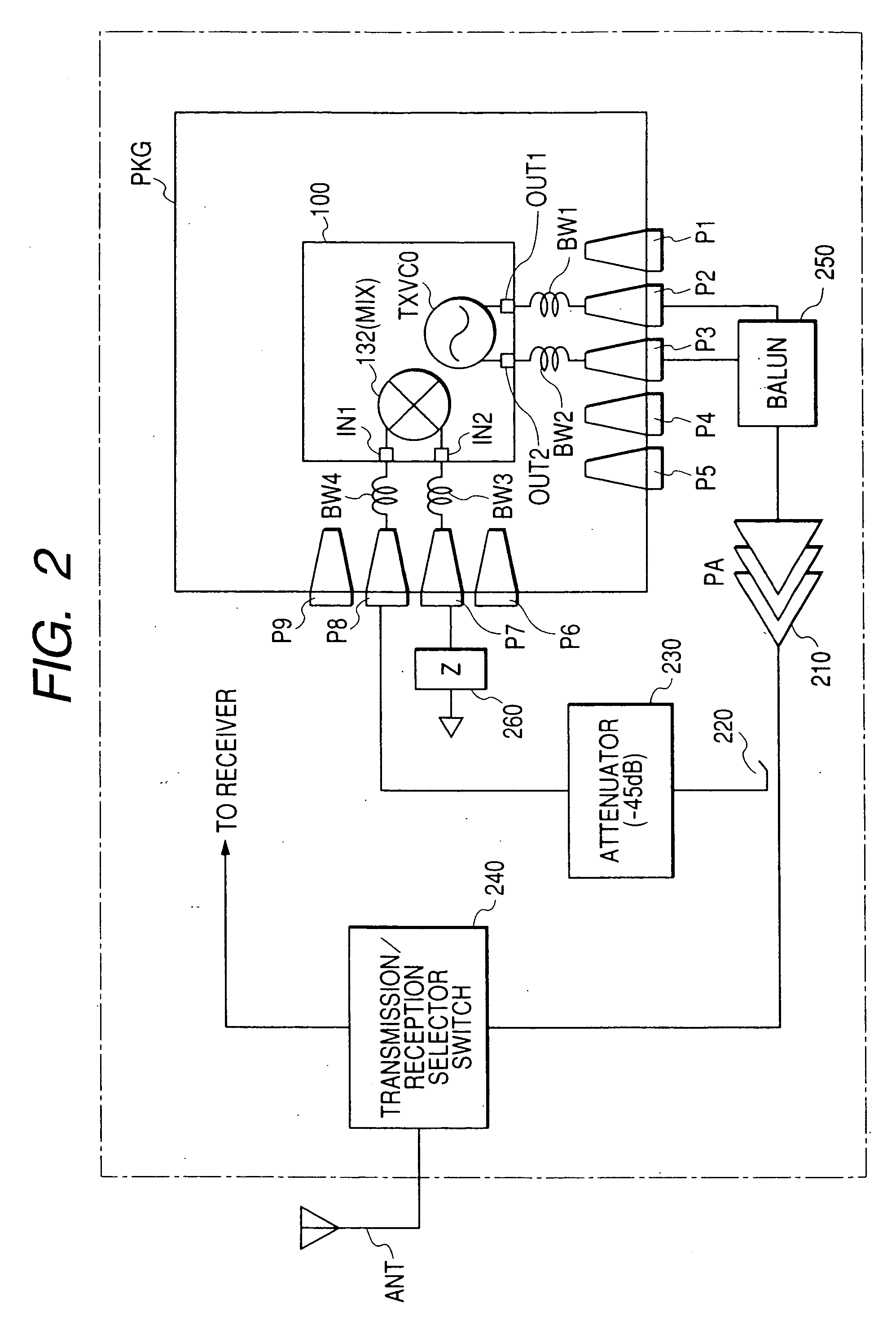
[0052] Next, referring to FIG. 2, the high frequency IC 100 according to the present invention wherein the transmission oscillator TxVCO is provided at its output end with anti-crosstalk measures will be described. Also, the constitution and action of a module mounted with the high frequency IC 100 will be described with reference to FIG. 2.

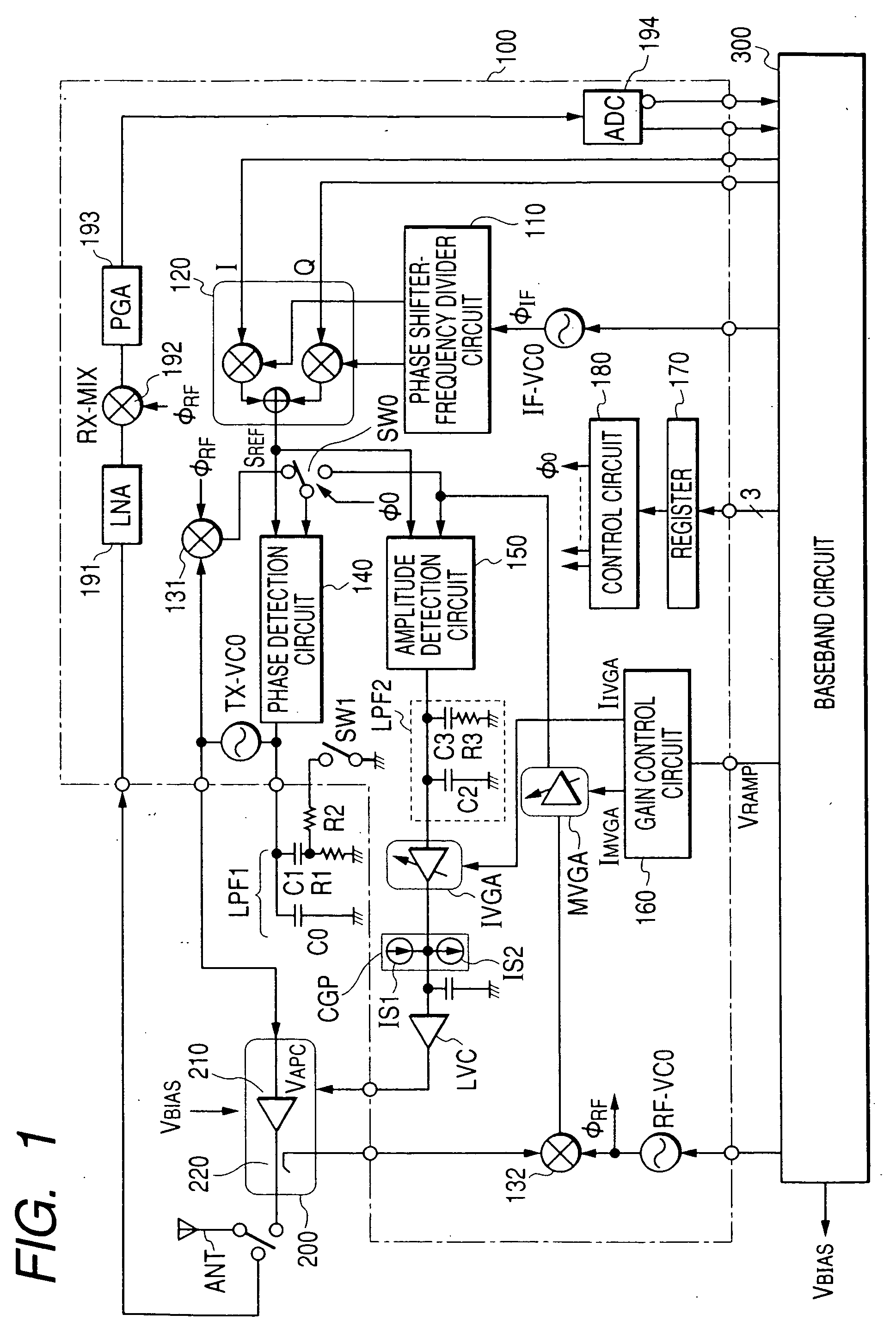
[0053]FIG. 2 illustrates what is constituted as a module by mounting the following elements over one insulating substrate, such as ceramic substrate: a high frequency IC 100 which constitutes the polar-loop transmitter wireless communication system in FIG. 1; a power amplifier 210; a coupler 220 which detects the output level of the power amplifier 210; an attenuator 230 which attenuates signals detected by the coupler 220; and a transmission / reception selector switch 240. The high frequency IC 100 is mounted as is sealed in a package. In this specification, the high frequency IC 100 sealed in a package is designated as high frequency semiconduct...

second embodiment

[0062] Next, referring to FIG. 3, the high frequency IC 100 according to the present invention wherein the transmission oscillator TxVCO is provided at its output end with anti-crosstalk measures will be described. Also, an RF module mounted with the high frequency IC 100 will be described. In FIG. 3, the same regions and circuits as in FIG. 2 will be marked with the same codes, and duplicate description will be omitted.

[0063] As mentioned above, the first embodiment is provided with the output terminal P3 for transmit signals in opposite phase. In the second embodiment, alternatively, an equivalent impedance circuit 261 is sealed in the package PKG of the high frequency IC. The equivalent impedance circuit 261 has an impedance equivalent to the impedance on the side of the output terminal P2 for transmit signals. That is, the equivalent impedance circuit 261 has an impedance equivalent to the impedance between the other end of the bonding wire BW1 connected with one output terminal...


PUM


Abstract

A transmission oscillator of differential output configuration is incorporated into a high frequency IC. Further, an equivalent impedance having an impedance equivalent to the impedance connected with a regular output terminal is provided. Or, a dummy external terminal for outputting transmit signals in opposite phase is provided. One of the differential outputs of the transmission oscillator is inputted to the power amplifier through the regular output terminal. The other of the differential outputs is connected to the equivalent impedance or the dummy external terminal.

Description

CROSS-REFERENCE [0001] This is a continuation application of U.S. Ser. No. 10 / 870,914, filed Jun. 21, 2004. [0002] The present application claims priority from Japanese patent application JP 2003-208334 filed on Aug. 22, 2003, the content of which is hereby incorporated by reference into this application.BACKGROUND OF THE INVENTION [0003] The present invention relates to a technology which is effectively applicable to the suppression of coupling noise or crosstalk from the output end of a transmission oscillator in a high frequency IC incorporating a transmission oscillator to other terminals. More particularly, the present invention relates to a technology which is effectively applicable to a high frequency semiconductor integrated circuit device and a wireless electric unit having a phase control loop for phase modulation and an amplitude control loop for amplitude modulation and a wireless communication system, such as cellular phone, incorporating the wireless electric unit. [00...

Claims


Application Information

Patent Timeline
Patent Type & Authority Applications(United States)
IPC IPC(8): H04B1/26H04B15/00H01L21/60H03C5/00H03L7/00H04B1/04
CPCH01L24/02H01L2924/01004H01L2924/01006H01L2924/01013H01L2924/01082H03C5/00H01L2924/01005H01L2924/1305H01L2924/13091H01L2924/01033H01L2924/00H01L2924/15787H01L2924/14H01L24/48H01L24/49
Inventor YAHAGI, KOICHIHIKASA, KAZUHIKOTAKANO, RYOICHI
Owner RENESAS ELECTRONICS CORP
Learn More