MOS varactor with segmented gate doping

Inactive Publication Date: 2007-02-08
IBM CORP
View PDF22 Cites 21 Cited by
  • Summary
  • Abstract
  • Description
  • Claims
  • Application Information

AI Technical Summary

Benefits of technology

[0006] The invention relates to a structure and method of fabrication of a MOS varactor whereby abutted p-n junctions in the polysilico

Problems solved by technology

This approach increases the total required a

Method used


Image

  • MOS varactor with segmented gate doping
  • MOS varactor with segmented gate doping
  • MOS varactor with segmented gate doping

Examples


Example

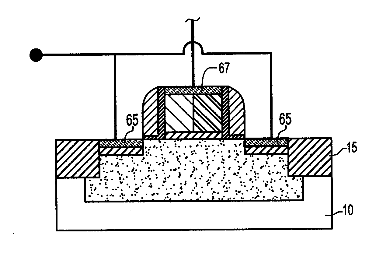
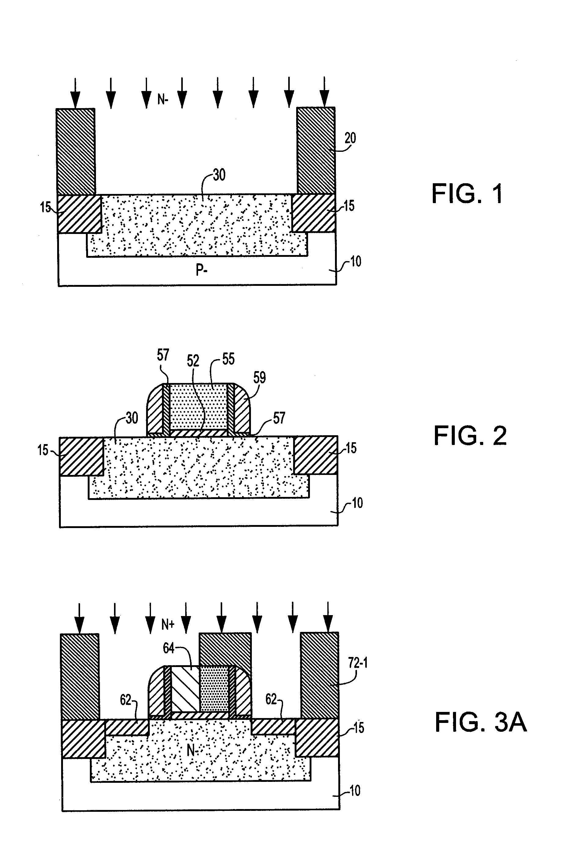
[0015]FIG. 1 shows a preliminary step in forming a varactor, in which a p-silicon substrate 10 is implanted with an N-well 30, using the same N− implant dose that is used elsewhere in the circuit to form N-wells. For convenience in the appended claims, the phrase “using the process dose for _X_” will be used to indicate that the element of the varactor in question uses the same dose, energy, etc as the referenced element in other circuit components, where the X denotes a well, a source or drain and the like. Photoresist 20 has been formed with an aperture exposing the area that will hold the varactor, overlapping with isolation 15, illustratively the same oxide shallow trench isolation as is used to isolate transistors. Well 30 will form the lower electrode of the varactor.

[0016]FIG. 2 shows the same area after a series of standard steps that include growing thermal oxide 52 simultaneously with the growth of gate oxides on FET transistors elsewhere in the circuit, depositing a laye...


PUM


Abstract

A MOS varactor is formed having a gate electrode comprising at least two abutting oppositely doped regions shorted together, in which the two regions are implanted simultaneously with source/drain implants for first and second types of transistor; at least one contact to a lower electrode is also formed simultaneously with the source/drain implants for the first type of transistor; the varactor insulator is formed simultaneously with the gate insulator for one type of transistor; and the lower electrode is formed simultaneously with a well for the first type of transistor, so that no additional mask is required.

Description

TECHNICAL FIELD [0001] The field of the invention is that of the fabrication of variable capacitors using integrated circuit techniques. BACKGROUND OF THE INVENTION [0002] Currently, the present MOS varactors have a limited tuning range which may also overlap positive and negative biases in order to encompass a complete tuning range as required by the circuit they are used in. [0003] Past implementations to improve the tuneability of a varactor have utilized separate n and p type gates wired in parallel. This approach increases the total required area and therefore is not an optimum solution. [0004] U.S. Pat. No. 6,667,539, to E. Alder, provides for a MOS varactor circuit having a pair of serially-connected varactors whose junctions are connected via a tap of a resistor to a resistor which is connected to adjacent terminals. [0005] Solutions that provide for MOS varactors with improved tuneability without impacting area, are of great value. SUMMARY OF THE INVENTION [0006] The invent...

Claims


Application Information

Patent Timeline
IPC IPC(8): H01L29/76H01L21/8234
CPCH01L27/0811H01L29/94H01L29/93H01L29/36
Inventor GREER, HEIDI L.KIM, SEONG-DONGRASSEL, ROBERT M.VAED, KUNAL
Owner IBM CORP
Why Eureka
Try Eureka