Solid-state image sensing device and method for fabricating the same

a solid-state image and sensing device technology, applied in the direction of radioation control devices, television system scanning details, television systems, etc., can solve the problems of changing some of the conforming devices to defective ones, and achieve the effects of reducing the amount of reflected light, preventing the occurrence of defects resulting from dust or the like, and enhancing the sensitivity of the solid-state image sensing devi

Inactive Publication Date: 2007-02-08
COLLABO INNOVATIONS INC
View PDF16 Cites 25 Cited by
  • Summary
  • Abstract
  • Description
  • Claims
  • Application Information

AI Technical Summary

Benefits of technology

[0035] With the present invention, the resin layer is interposed between the transparent substrate and a solid-state image sensing element composed of the light receiving unit, the microlens, the fluorine-containing resin material layer, and the like. In other words, unlike the conventional solid-state image sensing device, no air space is interposed between the transparent substrate and the solid-state image sensing element. Thus, the following effects can be exerted. That is to say, the phenomenon in which during delivery of the solid-state image sensing device, dust or the like moves from outside the solid-state image sensing element through the air space onto a pixel of the solid-state image sensing element is eliminated, so that the occurrence of defects resulting from this dust or the like can be completely prevented. Moreover, the reflectivity of light at the interface between the transparent substrate and the resin layer in the solid-state image sensing device of the present invention can be made smaller than that at the interface between the transparent substrate and the air space in the conventional solid-state image sensing device. Therefore, the sensitivity of the solid-state image sensing device can be enhanced. To be more specific, a decrease in the amount of reflected light between one side of the transparent substrate and the surface of the solid-state image sensing element can improve G-sensitivity (a wavelength of 550 nm) by about 8%. Furthermore, since the transparent substrate is directly adhered to the solid-state image sensing element, downsizing and reduction in height of the device can be attained as compared to the conventional solid-state image sensing device.
[0036] With the present invention, since the thickness of the resin layer is defined by the height of the spacer arranged around the area where the light receiving units are disposed (the pixel area), the thickness of the resin layer can be controlled to a desired value. Thus, for example, a thickened resin layer can attenuate α-ray, so that expensive, high-purity glass for α-ray attenuation does not have to be used as the transparent substrate. Consequently, fabrication costs can be reduced. Moreover, the spacer is provided along at least two facing sides of the pixel area in, for example, a quadrangular shape, which enables arrangement of the transparent substrate in parallel with the pixel area, that is, the image sensing surface. With this arrangement, in mounting the solid-state image sensing device of the present invention in a camera or the like, components can be installed using the top surface of the transparent substrate as the reference level. Therefore, the number of components installed between the reference level and a lens decreases as compared to the case where a member serving as the reference level is attached to the back surface of the package like the conventional solid-state image sensing device (see, for example, Patent Document 5: Japanese Unexamined Patent Publication No. 2005-51518). This reduces deviation of position for installing the components to improve the accuracy of image sensing. Furthermore, the arrangement of the transparent substrate in parallel with the pixel area, that is, the image sensing surface can certainly prevent color moiré, shading (non-uniform brightness), or the like. Moreover, the spacer is provided between the amplifier unit and the pixel area, and the spacer is formed with an opening not to face the amplifier unit. Thereby, when the transparent substrate is adhered with an adhesive serving as the resin layer to the fluorine-containing resin material layer, that is, to the semiconductor substrate, the spacer can inhibit a decrease in amplifier sensitivity due to the adhesive attaching to the amplifier unit.
[0037] As can be seen from the above, the present invention relates to solid-state image sensing devices having a solid-state image sensing element and a transparent substrate for protecting the element, and to their fabrication methods. When the present invention is applied to a CCD- or MOS-type image sensor or the like using a light-collecting microlens, or to a solid-state image sensing device to be mounted to a digital video camera, a digital still camera, a camera-equipped cellular telephone, or the like, a downsized solid-state image sensing device with high sensitivity can be provided stably at low cost. Accordingly, the present invention is very useful.

Problems solved by technology

This disadvantageously changes some of conforming devices to defective ones.

Method used


Image

  • Solid-state image sensing device and method for fabricating the same
  • Solid-state image sensing device and method for fabricating the same
  • Solid-state image sensing device and method for fabricating the same

Examples


first embodiment

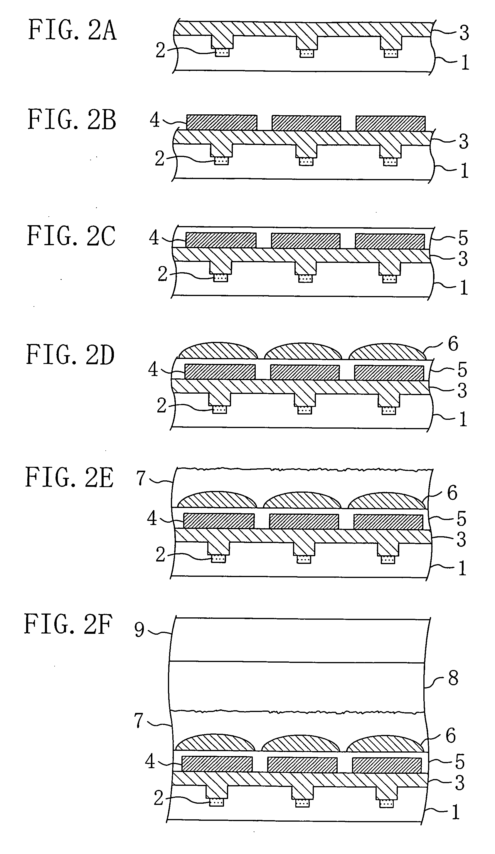
[0054] Hereinafter, a solid-state image sensing device and its fabrication method according to a first embodiment of the present invention will be described with reference to the accompanying drawings. Unless otherwise specified, the drawings illustrate the state of the device after a wafer is separated (diced) into the solid-state image sensing devices of individual element (chip) form.

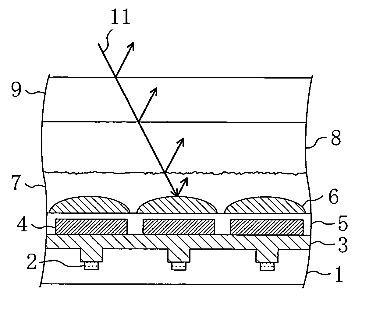
[0055]FIG. 1 shows a cross-sectional structure of the solid-state image sensing device according to the first embodiment. FIG. 1 concurrently shows how light comes in microlenses of the solid-state image sensing device according to the first embodiment.

[0056] Referring to FIG. 1, in the surface of a substrate 1 for a CCD-type solid-state image sensing element, a recess is provided on each pixel. At the bottom of the recess, a photodiode 2 is provided which converts an incoming light into an electrical signal. On the substrate 1 for the solid-state image sensing element, a first acrylic flattening f...

second embodiment

Modification of Second Embodiment

[0107] Hereinafter, a solid-state image sensing device and its fabrication method according to a modification of the second embodiment of the present invention will be described with reference to the accompanying drawings. As compared to the second embodiment, a characteristic of this modification is that a spacer in the present invention is provided between a pixel area and an amplifier unit arranged around the pixel area, and that the spacer is provided with an opening not to face the amplifier unit.

[0108]FIG. 12 exemplarily shows a schematic circuit structure of a solid-state image sensing device, specifically, an interline-transfer CCD solid-state image sensing device intended to apply this modification. As shown in FIG. 12, an image sensing region (pixel area) 63 of a CCD solid-state image sensing device 51 is composed of a plurality of light receiving units (photoelectric conversion units) 61 and a plurality of vertical transfer registers 62. ...


PUM


Abstract

A solid-state image sensing device comprises: a light receiving unit for receiving light; a microlens formed above the light receiving unit; a fluorine-containing resin material layer formed on the microlens; and a transparent substrate provided over the fluorine-containing resin material layer. A resin layer adheres the fluorine-containing resin material layer and the transparent substrate.

Description

BACKGROUND OF THE INVENTION [0001] (a) Fields of the Invention [0002] The present invention relates to solid-state image sensing devices having a solid-state image sensing element and a transparent substrate for protecting the element, and to their fabrication methods. [0003] (b) Description of Related Art [0004] In a solid-state image sensing device employing a CCD (Charge Coupled Device) and the like, the area of a photodiode serving as a light receiving unit has been decreasing by demands for downsizing and resolution enhancement thereof. Such a decrease in the area of the light receiving unit in turn degrades the light collection efficiency of the device. In order to make up for this degradation, a so-called microlens has come to be developed and then put into use. This microlens is typically made of resin and disposed above the light receiving unit formed on each pixel. The microlens refracts light not coming directly in the light receiving unit to collect the refracted light i...

Claims


Application Information

Patent Timeline
Patent Type & Authority Applications(United States)
IPC IPC(8): H04N5/225H01L27/14H04N5/335H04N5/369H04N5/372
CPCH01L27/14621H01L27/14623H01L27/14625H01L27/14627H04N5/335H01L27/14685H01L27/14687H01L27/14843H01L27/14868H01L27/14632H04N25/00H01L27/146
Inventor HIGUCHI, TOSHIHIROKOMATSU, TOMOKOMASUDA, TOMOKIHONJO, MAMORUTOMODA, NAOKI
Owner COLLABO INNOVATIONS INC
Why Eureka
Try Eureka