Optical module with flexible substrate

Inactive Publication Date: 2007-02-08
RENESAS ELECTRONICS CORP
View PDF5 Cites 13 Cited by
  • Summary
  • Abstract
  • Description
  • Claims
  • Application Information

AI Technical Summary

Benefits of technology

[0011] It is a main object of the present invention to improve the high-frequency characteristics.
[0018] With the present invention, it is possible to greatly increase the resonant frequency of the stub region of the bottom wiring layer of the flexible substrate, and thus it is possible to eliminate the problem of deteriorating high-frequency characteristics.

Problems solved by technology

When the stub region 134a on the bottom wiring layer 134 is eliminated, the stub structure disappears, however, when high-frequency current I flows to the wiring pattern 132a, a non-intentional line-shaped antenna or loop antenna is formed, and it becomes extremely easy for electromagnetic wave radiation to occur, which has an adverse effect on the external circuits.

Method used


Image

  • Optical module with flexible substrate
  • Optical module with flexible substrate
  • Optical module with flexible substrate

Examples


embodiment 1

(Embodiment 1)

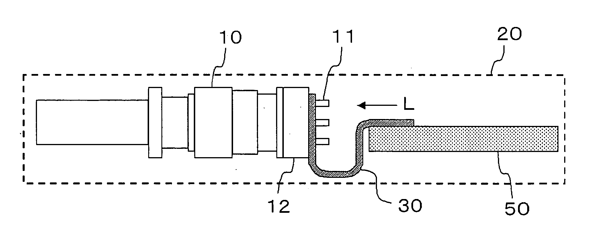
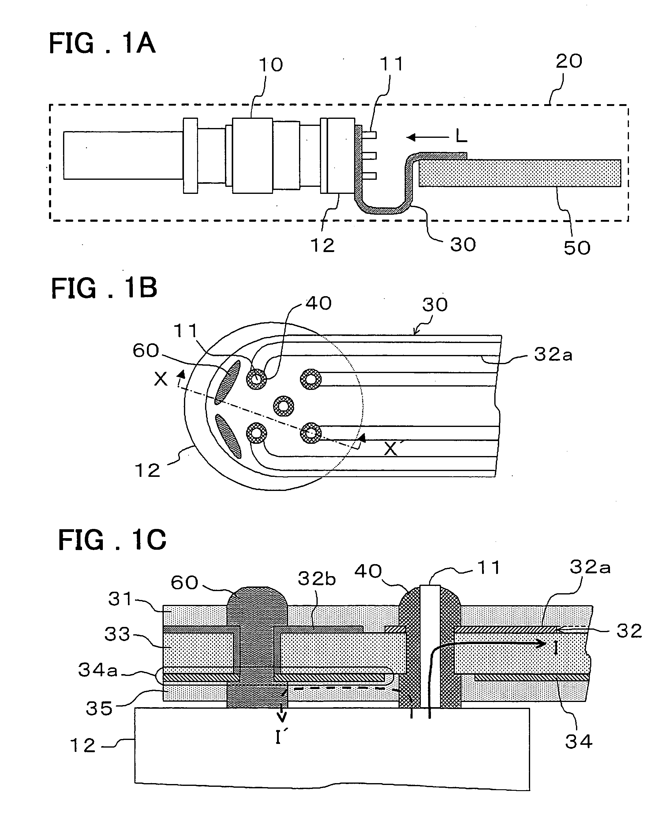
[0025] The optical transceiver of a first embodiment of the present invention will be explained using the drawings. FIGS. 1A, 1B and 1C are drawings showing the construction of the optical transceiver of a first embodiment of the present invention, where FIG. 1A is a side view of the inside of the housing, FIG. 1B is a view as seen from the direction of the arrow L, and FIG. 1C is a partial cross-sectional view of the section X-X′.

[0026] The optical transceiver is an optical transceiver with a flexible substrate in which an optical module 10 is electrically connected to a circuit board 50 by way of a flexible substrate 30, and it comprises: an optical module 10, housing 20, flexible substrate 30 and circuit board 50.

[0027] The optical module 10 is a device that converts an electrical signal to an optical signal, and with single-mode fiber (SMF) or multi-mode fiber (MMF) as a transmission path, transmits or receives data between communication devices, network devices,...

embodiment 2

(Embodiment 2)

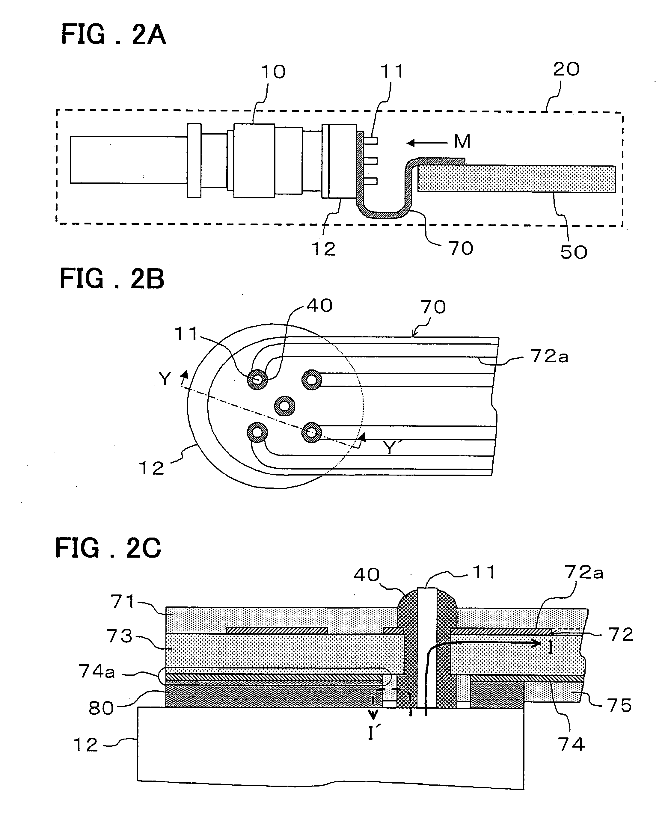
[0037] The optical transceiver of a second embodiment of the present invention will be explained using the drawings. FIGS. 2A, 2B and 2C are drawings showing the construction of the optical transceiver of a second embodiment of the present invention, where FIG. 2A is a side view of the inside of the housing, FIG. 2B is a view as seen from the direction of the arrow M, and FIG. 1C is a partial cross-sectional view of the section Y-Y′.

[0038] The construction of the flexible substrate 70 of the optical transceiver of this second embodiment differs from that of the first embodiment.

[0039] The flexible substrate 70 is constructed by forming a top wiring layer 72 and a bottom wiring layer 74 made of copper foil having a specified thickness on both sides of a polyimide layer 73 having a specified thickness, and covering the surface on the side of the top wiring layer 72 with a cover layer 71, and covering the surface on the side of the bottom wiring layer 74 with a cover la...

embodiment 3

(Embodiment 3)

[0045] An optical transceiver of a third embodiment of the present invention will be explained the drawings. FIGS. 6A, 6B and 6C are drawings showing the construction of the optical transceiver of the third embodiment of the present invention, wherein FIG. 6A is a side view of the inside of the housing, FIG. 6B is a view as seen from the direction of the arrow P, and FIG. 6C is a partial cross-sectional view of the section Q-Q′.

[0046] The optical transceiver of the third embodiment differs from that of the first embodiment in that the connecting points the solder 60 in the optical transceiver of the first embodiment are changed from two to three (or more). The other structure remains unchanged.

[0047] According to the third embodiment, the connecting points between the stem 12 and the bottom wiring layer 34 are increased, resulting in a further strengthening of the ground and an improved high frequency characteristics. The connecting area between the dummy wiring patt...


PUM


Abstract

An optical module with flexible substrate that improves high-frequency characteristics. A flexible substrate 30 is formed with a top wiring layer 32 and a bottom wiring layer 34 formed on both surfaces of a polyimide layer 33, where the top wiring layer 32 has a plurality of wiring patterns 32a that electrically connect the leads 11 of the optical module 10 to the drive circuit of a circuit board 50, and the bottom wiring layer 34 is located on the entire surface of one side of the polyimide layer 33 so that it is electrically insulated from the wiring patterns 32a, is electrically connected to the ground of the circuit board 50, and is electrically connected to at least the leads 11 and, depending on its relationship with the wiring patterns 32a, to the stem 12 of the optical module 10 at a specified position of a stub region 34a having stub structure.

Description

FIELD OF THE INVENTION [0001] This invention relates to an optical module with flexible substrate in which the optical module is electrically connected to a circuit board by way of a flexible substrate, and more particularly relates to an optical module with flexible substrate that is capable of improving high-frequency characteristics. BACKGROUND OF THE INVENTION [0002] In recent years, in optical transceivers 101 such as an XFP (10 Gbit Small Form Factor Pluggable) optical transceiver, an optical module 110 (light-receiving element, light-emitting element) is mounted inside a housing 120, and in order to maintain 10 Gbps-class high-frequency transmission characteristics, the optical module 110 is electrically connected to a circuit board 150 (board having a drive circuit) by way of a flexible substrate 130 (see FIG. 3, patent document 1). One reason for this kind of construction is that, as shown in FIG. 4, when the leads 111 of the optical module 110 are bent and electrically con...

Claims


Application Information

Patent Timeline
IPC IPC(8): G02B6/36G02B6/12G02B6/42H01L31/02H01S5/022H05K1/02
CPCG02B6/4201H05K1/0243H05K2201/10446H05K1/189H05K2201/10121H05K1/147G02B6/4283G02B6/4281G02B6/4279
Inventor MITAMURA, KAZUHIROWATANABE, ISAOITOH, HIDENORI
Owner RENESAS ELECTRONICS CORP
Why Eureka
Try Eureka