Magnetic field coupling element, antenna device, and electronic equipment
- Summary
- Abstract
- Description
- Claims
- Application Information
AI Technical Summary
Benefits of technology
Problems solved by technology
Method used
Image
Examples
first preferred embodiment
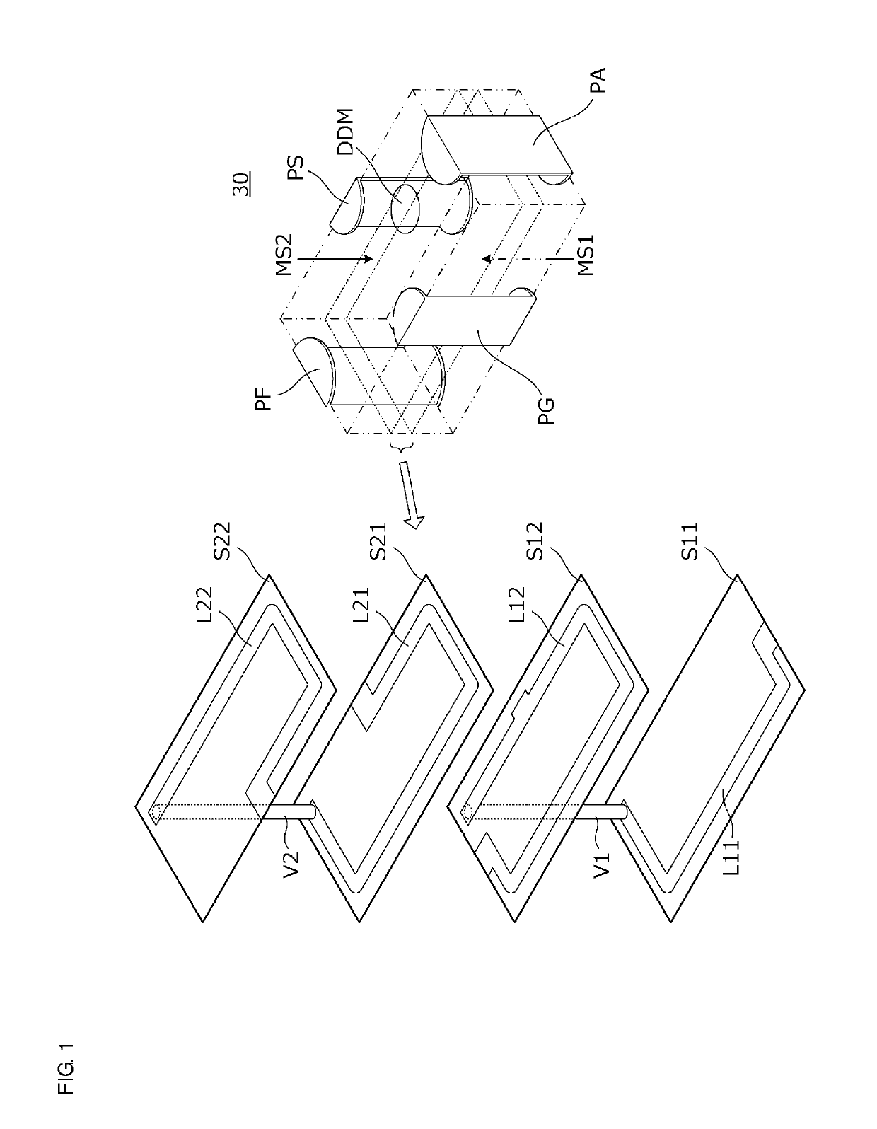
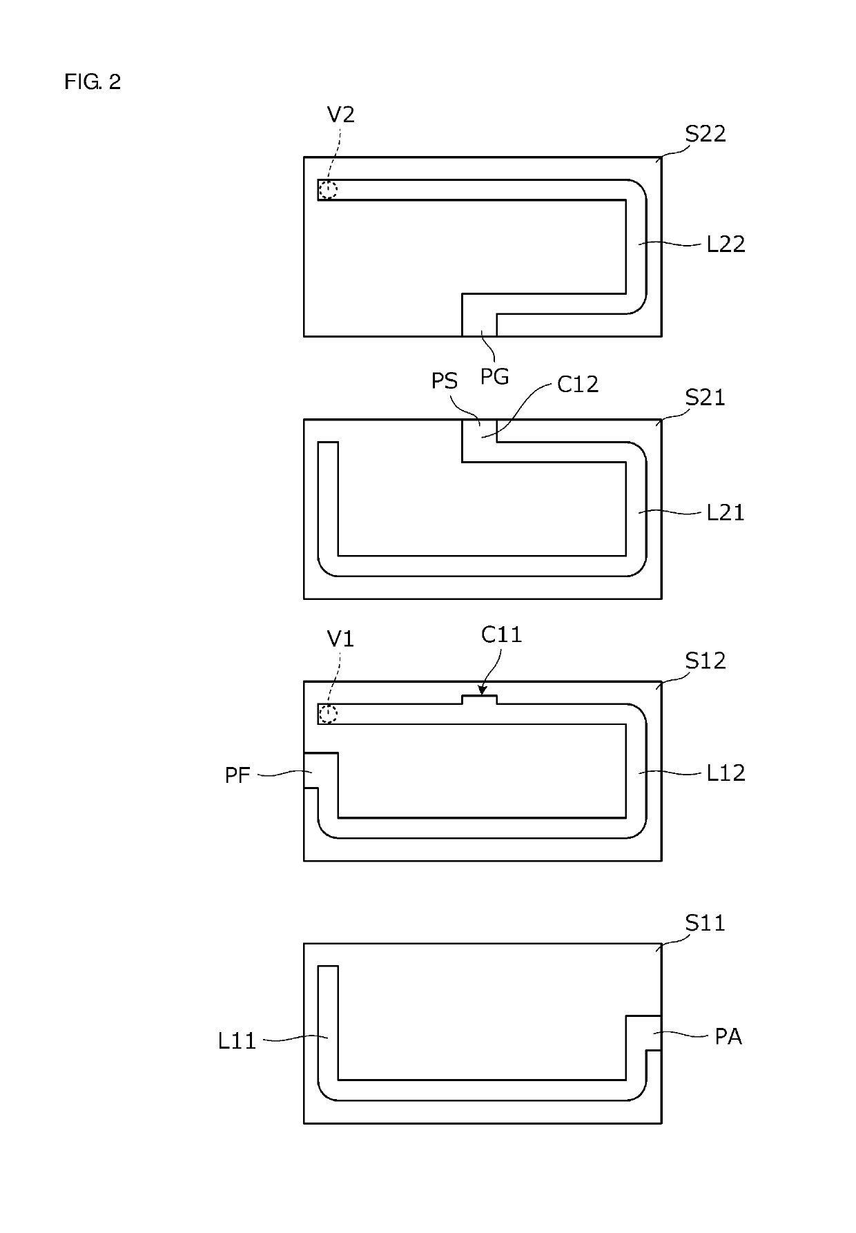
[0090]FIG. 1 is a perspective view of a coupling circuit 30 that is an example of the magnetic field coupling element according to a first preferred embodiment of the present invention. FIG. 2 is an exploded plan view illustrating conductor patterns provided on layers of the coupling circuit 30.
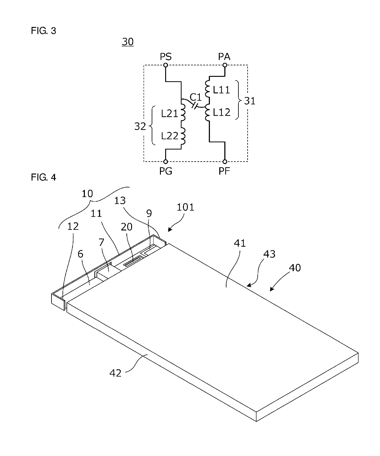
[0091]The coupling circuit 30 according to the present preferred embodiment is a rectangular or substantially rectangular parallelepiped chip component to be mounted on a circuit substrate in electronic equipment. In FIG. 1, an external structure of the coupling circuit 30 and an internal structure thereof are separately illustrated. The external structure of the coupling circuit 30 is represented by a two-dotted-and-dashed line. On an outer surface of the coupling circuit 30, a feeder circuit connection terminal PF, a radiating element connection terminal PA, a ground terminal PG, and a parasitic resonant circuit connection terminal PS are provided. In addition, the coupling circuit 30 inclu...
second preferred embodiment
[0143]FIG. 11 illustrates a circuit configuration of an antenna device 102 according to a second preferred embodiment of the present invention. In the antenna device 102, an inductor 35 is connected (inserted) between the second coil 32 of the coupling circuit 30 and the parasitic resonant circuit 20. The remaining configuration is the same or substantially the same as that of the circuit illustrated in FIG. 6 in the first preferred embodiment.
[0144]According to the present preferred embodiment, the inductor 35 is provided at a portion at which current is low. Thus, while a change in the coupling of the coupling circuit 30 is reduced or prevented, the resonant frequency of the parasitic resonant circuit 20 is able to be decreased, and a desired communication band is able to be obtained. Alternatively, while the resonant frequency is maintained, the length of the parasitic resonant circuit 20 is able to be reduced, and the area used is reduced.
[0145]Note that the inductor 35 may also...
third preferred embodiment
[0146]FIG. 12 illustrates a circuit configuration of an antenna device 103 according to a third preferred embodiment of the present invention. In the antenna device 103, the inductor 35 is connected (inserted) between the second coil 32 of the coupling circuit 30 and the ground. The remaining configuration is the same or substantially the same as that of the circuit illustrated in FIG. 6 in the first preferred embodiment.
[0147]When the coupling circuit 30 is added to the antenna device, a parasitic capacitance is generated between the ground and the coupling circuit 30. According to the present preferred embodiment, resonance between the inductor 35 and the parasitic capacitance is able to reduce or prevent a reactance component. Therefore, in a frequency band in which an antenna characteristic is not desired to be changed by the addition of the coupling circuit 30 to the antenna device, by including the inductor 35 with such an inductance as to resonate with the parasitic capacitan...
PUM
 Abstract
Description
Claims
Application Information


