An electrostatic discharge circuit

a technology of electrostatic discharge and circuit, applied in the direction of diodes, semiconductor devices, semiconductor/solid-state device details, etc., can solve the problems of serious problems with esd circuits, circuits operating below 8 v cannot be protected, and parts or total loss of normal functions, etc., to achieve better esd protection, improve esd protection, and improve the effect of esd protection

Inactive Publication Date: 2007-02-22
SILICON MOTION INC (TW)
View PDF4 Cites 2 Cited by
  • Summary
  • Abstract
  • Description
  • Claims
  • Application Information

AI Technical Summary

Benefits of technology

[0013] Another objective of the invention is to provide an ESD zener diode which can be used in an ESD circuit to lower its breakdown voltage, thus providing better ESD protection.
[0014] According to a preferred embodiment of the invention, the ESD circuit includes an NMOS transistor, a PMOS transistor, and an ESD zener diode. The ESD zener diode is used to decrease the breakdown voltage, so that the electrical current discharges through it, thereby preventing the circuit from burning out and also greatly enhancing the function of ESD protection.

Problems solved by technology

Such static electricity may not have great influence on human bodies, but it may cause damage to some devices that are sensitive to electrostatic effects so that they partially or totally lose their normal functions.
However, there is a very serious problem with these ESD circuits.
That is, the breakdown voltages of these ESD circuits are about 8-10 V. In other words, they cannot provide any protection for circuits operating below 8 V.

Method used


Image

  • An electrostatic discharge circuit
  • An electrostatic discharge circuit
  • An electrostatic discharge circuit

Examples


Embodiment Construction

[0021] The present invention will be apparent from the following detailed description, which proceeds with reference to the accompanying drawings, wherein the same references relate to the same elements.

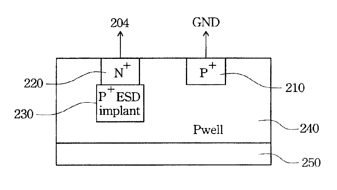
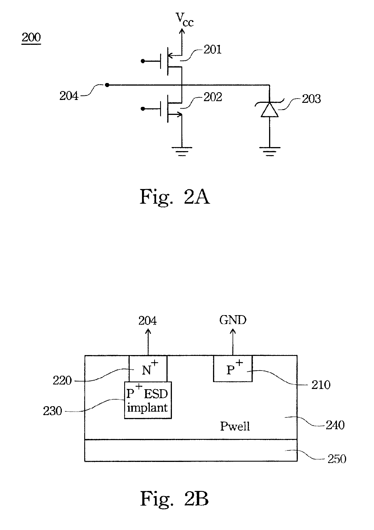
[0022] A preferred embodiment of the disclosed ESD circuit 200 is shown in FIG. 2A. The circuit 200 includes an NMOS transistor 202, a PMOS transistor 201, and an ESD zener diode 203. The source of the PMOS transistor 201 is coupled to a high voltage Vcc. The drain of the NMOS transistor 202 is simultaneously coupled to a circuit device terminal 204, the drain of the PMOS transistor 201, and the cathode of the ESD zener diode 203. The anode of the ESD zener diode 203 is coupled to the ground. When a normal positive voltage Vcc is imposed on the NMOS transistor 202 and the PMOS transistor 201, the NMOS transistor 202 and the PMOS transistor 201 are electrically coupled. However, if the transistor malfunctions or static electricity is produced, the high voltage is discharged via the E...


PUM


Abstract

An electrostatic discharge circuit includes at least an electrostatic discharge zener diode, an NMOS transistor, and a PMOS transistor. The electrostatic discharge zener diode is used for lowering the breakdown voltage and making the electrical current discharge through it, thereby preventing the circuit device from burning out and greatly enhancing the function of electrostatic discharge protection.

Description

CROSS-REFERENCE TO RELATED APPLICATIONS [0001] The present application is based on, and claims priority from, Taiwan Application Serial Number 94128101, filed Aug. 17, 2005, the disclosure of which is hereby incorporated by reference herein in its entirety. BACKGROUND OF THE INVENTION [0002] 1. Field of Invention [0003] The invention relates to an electrostatic discharge (ESD) circuit and, in particular, to an ESD circuit using the ESD zener diode. [0004] 2. Related Art [0005] In daily life, separating different materials from or rubbing different materials against each other can produce static electricity. For example, squeezing, cutting, moving, churning, and filtering in production processes; and walking, standing, and taking off clothes in daily life all produce static electricity. One therefore may say that static electricity is everywhere. Even our bodies and surroundings may carry a lot of electrostatic voltage, up to thousands or even tens of thousands of volts. Such static ...

Claims


Application Information

Patent Timeline
Patent Type & Authority Applications(United States)
IPC IPC(8): H01L23/62
CPCH01L27/0255
Inventor CHEN, TE-WEIWENG, LI-CHIU
Owner SILICON MOTION INC (TW)
Why Eureka
Try Eureka