Method of packaging and interconnection of integrated circuits

a technology of integrated circuits and interconnections, applied in the field of electronic packaging, can solve the problems of bump forming cost, cost and technical limitations are significant, and the overall cost is saved

Inactive Publication Date: 2007-02-22
TERECIRCUITS CORP
View PDF20 Cites 45 Cited by
  • Summary
  • Abstract
  • Description
  • Claims
  • Application Information

AI Technical Summary

Benefits of technology

[0011] The present invention provides an IC packaging concept in which the surface of the IC chips is coplanar with the surface of the substrate in which it is embedded, and to have no gaps between the side of the IC chips and the substrate. In this way, interconnect metal lines can be easily placed on this uninterrupted surface, connecting the various chips or other components.

Problems solved by technology

In addition, flip-chip bonding requires minimal mounting area, which results in further overall cost saving.
However, its costs and technical limitations are significant such as bump forming cost, underfilling manufacturing complexity and cost, long term reliability cost due to thermo-mechanical stresses, and environmental cost.
However, the performance of such devices tends to be less than optimal, and the processes for fabricating them less well developed and more costly than for the well-known processes of fabricating transistors in silicon wafers.
In practice, many problems arise in the handling of such thin (and therefore delicate) chips.
However, apart from the possibility of defects arising from incomplete filling of the holes, this process does not result in a highly planar surface due to variations 12 in the thickness of chips coupled with variations in the depth of the depressions, and there is still a small but significant gap 13 between the side of the chip and the side of the hole.
This leads to complexity in forming the subsequent interconnect metallization.
It also does not address the issue of mismatched CTEs.
However, as with the Fluidic Self-Assembly process, there would still be imperfections in the coplanarity due to the inevitable variations, and there would still be a gap between the sides of the chip and the side of the cutout.

Method used


Image

  • Method of packaging and interconnection of integrated circuits
  • Method of packaging and interconnection of integrated circuits
  • Method of packaging and interconnection of integrated circuits

Examples


Embodiment Construction

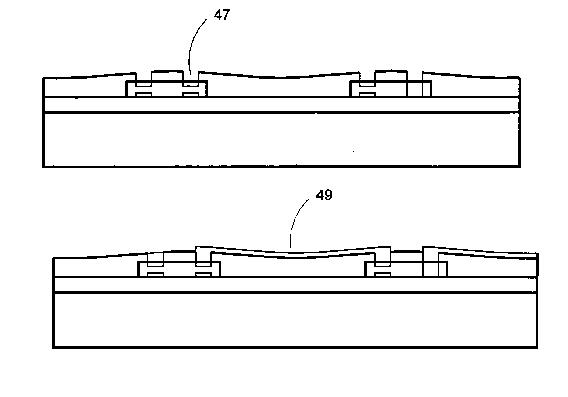
[0022] The present invention provides an IC packaging concept in which the surfaces of the embedded IC chips are coplanar with the complete structure with no side gaps to allow uninterrupted interconnect metal lines. The packaging concept further employs an interposer of low CTE between the IC chips and the substrate to improve interconnection reliability due to thermal cycling.

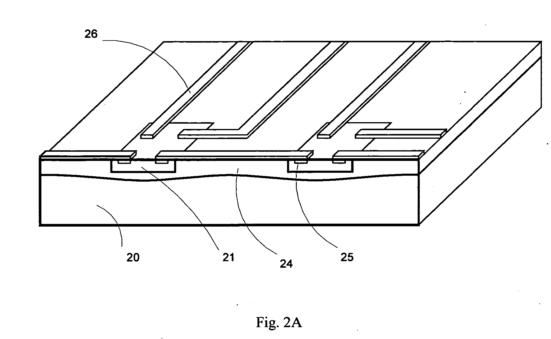
[0023]FIG. 2A shows an embodiment of the structure of the present invention. A plurality of IC chips 21 is embedded in a substrate 20 through a casting layer 24. The IC chips contain top exposed contact pads 25, which can be connected to each other or to other external circuitry by conductive interconnect 26. One of the novel results of the present invention packaging structure is to have the surface of the IC chip 21 coplanar with the surface of the complete structure in which it is embedded, and to have no gaps between the side of the IC and the substrate. In this way, interconnect metal lines can be easil...


PUM


Abstract

A method is disclosed for packaging semiconductor chips on a flexible substrate employing thin film transfer. The semiconductor chips are placed on a temporary adhesive substrate, then covered by a permanent flexible substrate with a casting layer for planarizingly embedding the chips on the permanent substrate before removing the temporary substrate. With the surface of the chips coplanar with the surface of the complete structure without any gaps, interconnect metal lines can be easily placed on the uninterrupted surface, connecting the chips and other components.

Description

FIELD OF THE INVENTION [0001] The present invention is related generally to electronics packaging and, more particularly to packaging and interconnection of integrated circuits on a flexible substrate. BACKGROUND OF THE INVENTION [0002] Board level semiconductor packaging and interconnection of integrated circuits (IC) is the process to electrically connect the IC chips to each other and to external circuitry to function as an electronic system. The IC chips have input and output contact pads and the interconnection is typically an array of metallic connections within a support substrate. The normal packaging process of forming a fully functional product based on integrated circuits usually includes placing the semiconductor IC chips on a printed circuit board (PCB) and soldering their contact pads to contact pads on the PCB. Several connection techniques are widely used and well known in the art. These include wire bonding, tape automated bonding (TAB), flip-chip bonding, etc. [000...

Claims


Application Information

Patent Timeline
Patent Type & Authority Applications(United States)
IPC IPC(8): H01L23/02
CPCH01L23/5389H01L24/24H01L24/25H01L24/82H01L2224/24137H01L2224/24227H01L2224/2518H01L2224/76155H01L2224/82039H01L2924/01027H01L2924/01079H01L2924/01082H01L2924/10253H01L2924/14H01L2924/15153H01L2924/15165H01L2924/19041H01L2924/19042H01L2924/19043H01L2924/01033H01L2924/014H01L2224/73267H01L2224/82102H01L2224/32225H01L2224/92244H01L2224/24101
Inventor SHEATS, JAMES
Owner TERECIRCUITS CORP
Why Eureka
Try Eureka