Ion implanted insulator material with reduced dielectric constant

a technology of insulator material and dielectric constant, which is applied in the direction of chemical vapor deposition coating, semiconductor/solid-state device details, coatings, etc., can solve the problems of low dielectric constant of porous materials with low dielectric constant, poor mechanical properties of silicon dioxide, and low dielectric constant of silicon dioxide, so as to reduce the dielectric constant

Inactive Publication Date: 2007-02-22
AL BAYATI AMIR +7
View PDF99 Cites 39 Cited by
  • Summary
  • Abstract
  • Description
  • Claims
  • Application Information

AI Technical Summary

Benefits of technology

[0007] An integrated microelectronic circuit has a multi-layer interconnect structure overlying the transistors consisting of stacked metal pattern layers and insulating layers separating adjacent ones of said metal pattern layers. Each of the insulating layers is a dielectric material with plural gas bubbles distributed within the volume of the dielectric material to reduce its dielectric constant, the gas bubbles being formed by ion implantation of a gaseous species into the dielectric material.

Problems solved by technology

Due to the large number of interconnect layers and the total electrical path length they represent, the interconnect layers account for a significant proportion if not a majority of the total power losses in the integrated circuit.
However, silicon dioxide has a relatively high dielectric constant (about 4.0) and is therefore not ideal.
Unfortunately, their mechanical properties are inferior to those of silicon dioxide because these materials tend to be porous and therefore are not as hard as silicon dioxide.
This is a particularly difficult problem because the insulator layer deposited over an interconnect layer tends to form a very uneven top surface and must therefore be smoothed to a plane surface by chemical mechanical polishing.
While silicon dioxide is a sufficiently hard material to be relatively impervious to flaking or cracking during chemical mechanical polishing, porous materials with low dielectric constant can be susceptible to damage during chemical mechanical polishing.

Method used


Image

  • Ion implanted insulator material with reduced dielectric constant
  • Ion implanted insulator material with reduced dielectric constant
  • Ion implanted insulator material with reduced dielectric constant

Examples


Embodiment Construction

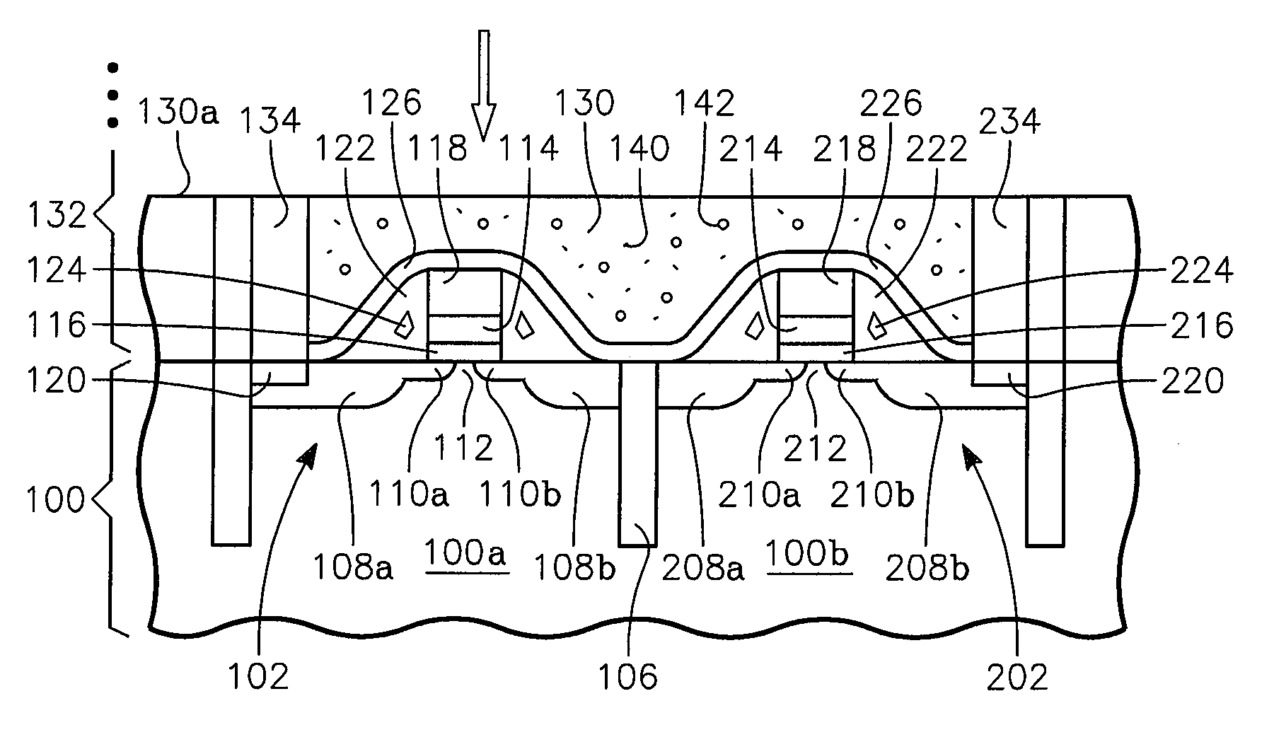
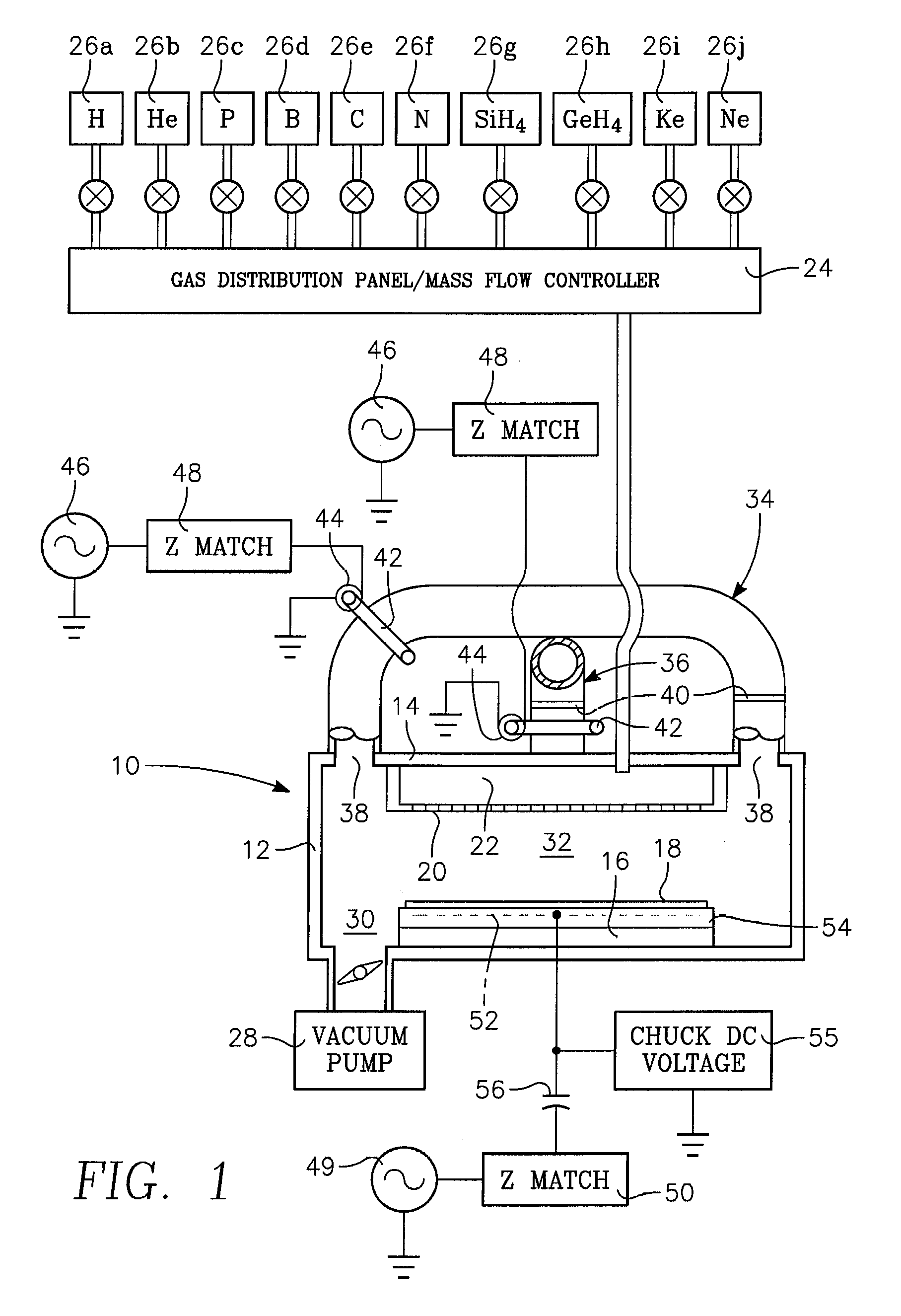
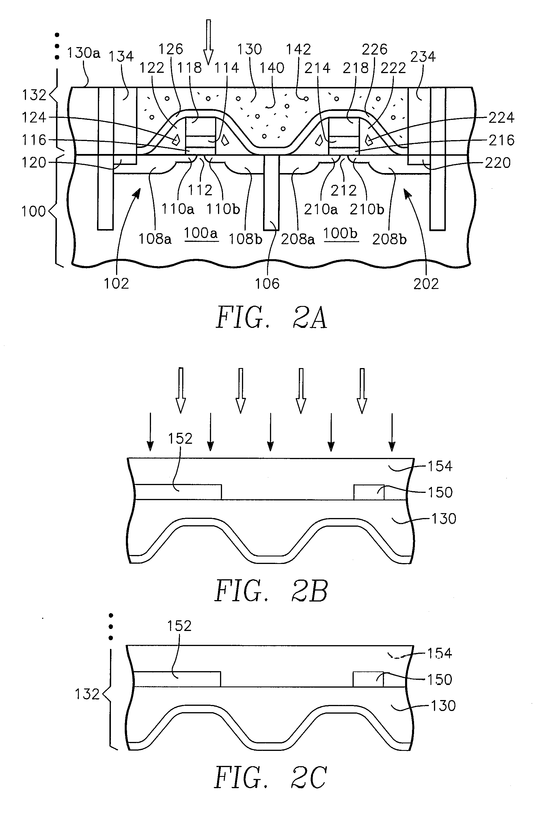
[0027] In the present invention, an insulating material having excellent mechanical properties but poor electrical properties (a relatively high dielectric constant) is subject to ion implantation of a light gaseous species such as hydrogen or helium. The ion energy and dosage of the implantation process and the temperature of the insulating material are selected so that implanted atoms of the gaseous species inside the insulating material migrate or coalesce toward one another to form small gas bubbles throughout the insulating material. The gas bubbles within the insulating material have a very low dielectric constant (e.g., about 1.04). The result is that the total dielectric constant of the insulating layer is significantly reduced due to the presence of the bubbles. In the case of silicon dioxide containing bubbles formed by ion implantation of a gaseous species, the dielectric constant may be as low as 3.5. The reduction in dielectric constant depends upon the proportion of th...


PUM

PropertyMeasurementUnit
diameteraaaaaaaaaa
diameteraaaaaaaaaa
average diameteraaaaaaaaaa

Abstract

An integrated microelectronic circuit has a multi-layer interconnect structure overlying the transistors consisting of stacked metal pattern layers and insulating layers separating adjacent ones of said metal pattern layers. Each of the insulating layers is a dielectric material with plural gas bubbles distributed within the volume of the dielectric material to reduce the dielectric constant of the material, the gas bubbles being formed by ion implantation of a gaseous species into the dielectric material.

Description

CROSS-REFERENCE TO RELATED APPLICATIONS [0001] This application is a divisional of U.S. divisional application Ser. No. 11 / 003,000 filed Dec. 1, 2004 entitled METHOD FOR ION IMPLANTING INSULATOR MATERIAL TO REDUCE DIELECTRIC CONSTANT, by Amir Al-Bayati, et al., which is a continuation-in-part of U.S. application Ser. No. 10 / 838,052 filed May 3, 2004 entitled LOW TEMPERATURE CVD PROCESS WITH CONFORMALITY, STRESS AND COMPOSITION by Hiroji Hanawa, et al., the disclosure of which is incorporated herein by reference and of which is a continuation-in-part of U.S. patent application Ser. No. 10 / 786,410 filed Feb. 24, 2004 entitled FABRICATION OF SILICON ON INSULATOR STRUCTURE USING PLASMA IMMERSION ION IMPLANTATION by Dan Maydan et al., which is a continuation-in-part of U.S. patent application Ser. No. 10 / 646,533 filed Aug. 22, 2003 entitled PLASMA IMMERSION ION IMPLANTATION PROCESS USING A PLASMA SOURCE HAVING LOW DISSOCIATION AND LOW MINIMUM PLASMA VOLTAGE by Kenneth Collins et al., whi...

Claims


Application Information

Patent Timeline
Patent Type & Authority Applications(United States)
IPC IPC(8): H01L21/425
CPCC23C16/56H01L21/02126H01L21/02203H01L21/02211H01L21/02274H01L21/02321H01L21/0234H01L21/31695H01L21/7682H01L21/76825H01L21/823864H01L21/823871H01L23/5329H01L23/53295H01L2924/3011H01L2924/0002H01L2924/00H01L2221/1047
Inventor AL-BAYATI, AMIRROBERTS, RICK J.COLLINS, KENNETH S.MACWILLIAMS, KENHANAWA, HIROJIRAMASWAMY, KARTIKGALLO, BIAGIONGUYEN, ANDREW
Owner AL BAYATI AMIR
Why Eureka
Try Eureka